
Everyone is talking about FinFETs - it can be said that this is the biggest change in transistors since the commercialization of MOSFETs in 1960. Almost everyone - except those who are still enthusiastic about fully depleted insulator silicon thin films (FDSOI), believes that FinFETs will be the future of SoCs after 20 nm. But what about the future for system developers who want to use these SoCs?
The best way to answer this question is to say what FinFET means for analog and digital circuit designers and SoC designers. From this information, we can deduce what the FinFET means at the system level.
What is the difference between FinFET?
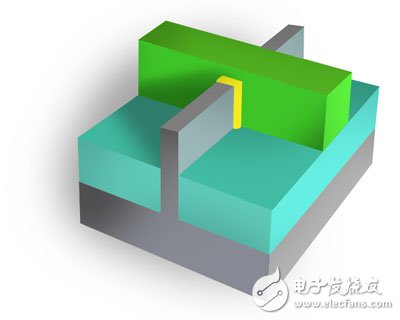
There has been a lot of discussion about the theory of FinFETs and their structures (Figure 1), and we won't repeat these discussions here. From a circuit designer's point of view, we are more concerned about how FinFETs differ from planar MOSFETs. Regarding this issue, this year's Design Automation Conference (DAC) technical discussion topic opened up new ideas for analog designers.
Figure 1. FinFET is often found in a variety of materials.
"FinFET for analog design" instead of ridiculously saying "God must be crazy", which represents the views of four experts: foundry line represents TSMC's Eric Soenen, Globalfoundries' Richard Trihy, tool expert Synopsys' Navraj Nandra, and Design manager Freescale's Scott Herrin. The discussion focused on the electrical characteristics of the new transistor.
On the pro side, Herrin pointed out that FinFET can achieve high gain with very low subthreshold leakage current.
Nandra added, "FinFET inherently has a high gain, but the transconductance (gm) is actually very low, just like the frequency (ft). More advanced geometry layouts are easier to match than planar devices, and transistor characteristics are well controlled. As a result, you can develop circuits with better performance. And, there are other amazing things. For example, the output current is small, so the data converter you develop will be smaller."
But there are also challenges. Nandra says that gm and gd are lower, and the gate leakage is larger, and the gate capacitance is twice as large as the planar device of the same size. As Soenen points out, it is known that the FinFET gate width is quantized: each transistor on the wafer has the same nominal gate width. Therefore, analog designers accustomed to using w-values ​​for each transistor can only use a set of identical FinFETs in parallel—in fact, w as a circuit parameter can be a continuous variable up to a set of positive integers.
Layout problem
Quantization changes the layout habit by replacing multiple width-adjustable transistors with multiple minimum-width transistors. For example, Synopsys has a tool that converts the gate width ratio to the number of fins required, Nanda said. But in another discussion group discussion, Anirudh Devgan, vice president of wafer process at Cadence, presented a more serious layout problem.
Devgan said: "With more advanced geometric layouts, multi-modes are more complicated. As complexity increases, it is difficult to predict design rule errors. Errors are related to the environment."
Some rules are familiar: for example, reducing the spacing rules of coupling, the shape rules of lithography, and the like. Dual mode adds color rules to ensure that the finest mode can be split into two separate masks. There are also relatively new layout-related effects, and Devgan points out six of them—including very close and multiple intervals—that have a large impact on transistor behavior. To illustrate the seriousness of the problem, Devgan pointed out that there are already 5,000 layout rules at 20 nm that need to be checked.
For analog designers and digital cell library developers, the result is that it is almost impossible to develop a clean layout of the DRC structure. Designers must predict multiple iterations due to layout problems caused by extraction and DRC. Devgan reminded: "It takes a few weeks. 40% of the design time is spent on convergence."
Modeling challenge
In addition to these differences in transistor behavior, circuit designers have encountered other problems with FinFETs: the simulation model is structurally different from planar MOSFETs (Figure 2). Trihy reminds, “If you look at the model, the number of stray capacitance increases tenfold. It is not clear whether the desktop-driven emulator can handle FinFETs.â€
Figure 2. The FinFET simulator model can be very complicated
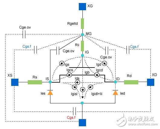
Even if it is so complicated, not all models are correct under all conditions. Therefore, for users unfamiliar with planar transistors, the choice of model will be related to the circuit and may also be related to the layout. Herrin agrees, “There is a difference, you must know the limitations of the model.â€
Nandra said that Synopsys has been using a combination of SPICE and TCAD process models, as well as the BSIM-4 common multi-gate model to achieve accurate simulation of FinFET circuits. He said that even in the sub-threshold area, BSIM-4 did implement an accurate behavioral model. However, when used in circuit simulation, the model can be very complicated. Nandra admits, "You must use a structure-related approach to solve the spur problem."
Trihy continues this theme. He asked, "Where does the device model stop, where do you start extracting circuits? With FinFET circuits, the boundaries are blurred. You can rely on design rules to limit interaction, but in the end, the most important thing is probably not the accuracy of the model. It is the precision of the extraction." In his speech, Devgan warned that in some cases, it may be necessary to solve the problem in the field, and to accurately extract the complex tightly packed 3D structure, the FinFET circuit will have this structure.
New method, new circuit
Transistor behavior, layout rules, and modeling methods have changed dramatically, so circuit topologies for 28 nm planar processes are unlikely to be used in 14 nm FinFET processes. Quantification brings some challenges. Low voltage, limited gm, and large gate capacitance can cause other changes, including limiting fanout, processing compression dynamic range, and more. Soenen warns, “This is not a power supply technology, but we plan to offer a 1.8 V FinFET,†Herrin explained. For example, in embedded applications, voltage limiting means completely different ESD circuits, using new methods to support high voltage I/ O.
Soenen and Nandra agree on the impact of these changes. Soenen predicts: "You will see a lot of digital auxiliary content in the analog circuit. You will see switched-capacitor filters and more oversampling techniques."
Nandra added, "We saw circuits that were not available before FinFET."
Chip level
For analog circuit and digital cell library designers, small size FinFETs have both advantages and disadvantages. The advantages are smaller circuits, higher operating frequencies, no need to worry too much about process variations, and of course lower subthreshold leakage. The downside is that design is more difficult and requires more iterations to achieve convergence. In general, the previous generations of designs cannot be reused. Designers have to build new circuit methods, topologies, and layouts. The new design means longer time, greater risk, speed, density and power consumption at the transistor level may be lost.
It is completely different for chip-level designers who use modules and cell libraries. Small size FinFETs are only more complex in modules and units. Chip designers often notice smaller, faster modules that have very low static power consumption. Finally, many designs are easier to implement for power management than previous products.
But there are still problems. Lower operating voltages make signal and power integrity analysis even more important. For synthesis logic, lower fanouts complicate timing closure. More difficult convergence at the module level means be very careful in the final integration phase, don't break anything. But these are very familiar issues, and each new process has these problems. This is of course unpopular.
to sum up
Finally, what does this mean for designers who will use FinFET-based SoC systems? Through our analysis here, and taking into account the application experience of Intel 20 nm tri-gate SoC in the industry, the same conclusion is reached.
Every successive step in the design chain—from transistors to cells or circuits, from circuits to functional blocks, from modules to chips, from chips to systems—the trend is to take advantage of FinFETs and overcome challenges. Chip designers get faster, less leaky libraries and don't need to know how cell designers develop them.
Similarly, system designers will see chips with higher component densities - depending on the structure, metal or polyethylene spacing, contact spacing or gate length reduces the area, which improves performance and effectively reduces leakage. Current. There may be some second-order effects. For example, a significantly lower core voltage places new demands on the voltage regulator, requiring noise reduction and good transient response. Some SoCs may not support traditional high voltage I/O.
In short, for system developers, the FinFET revolution is as saying: density, speed and power consumption have changed dramatically. There is a more interesting point. Asking circuit designers—especially analog designers—to abandon familiar circuits, FinFETs drive key innovations at the circuit level. The new circuit will drive some SoCs to shine in new open applications.
Trench Cover,Trench Drain,Drain Cover,Steel Trench Covers
Hunan Furui Mechanical and Electrical Equipment Manufacturing Co., Ltd. , https://www.thresher.nl