
The basic idea of ​​active noise control was first proposed by the German physicist Paul Lueg when he invented the "electronic muffler" in 1936. Compared with the traditional passive control, the active noise control technology has the advantages of obvious noise control effect on the medium and low frequency bands, light system and strong real-time performance, and has potential engineering application value. Noise control is real-time control, which requires a large amount of calculation, which is difficult to achieve with ordinary single-chip microcomputers. In the 1980s, the basic idea of ​​active control of digital signal processing (DSP) chips was first proposed by German physicist Paul Lueg when he invented the "electronic muffler" in 1936. Compared with the traditional passive control, the active noise control technology has the advantages of obvious noise control effect on the medium and low frequency bands, light system and strong real-time performance, and has potential engineering application value.
This article refers to the address: http://
Noise control is real-time control, which requires a large amount of calculation, which is difficult to achieve with ordinary single-chip microcomputers. In the 1980s, the advent of digital signal processing (DSP) chips opened up a vast space for real-time control of signals. With the continuous maturity and development of chip technology, DSP has become a core component of modern intelligent controllers.
In this paper, the DSP chip TMS320F2812 is used to design an intelligent controller that can run offline and independently and can be simulated online through USB interface. The vehicle internal noise active intelligent control system is designed with the controller as the core.
Circuit design of intelligent control system
1 Design process and system block diagram
The design process of the vehicle interior noise intelligent control system is shown in Figure 1.
DSP intelligent controller hardware design flow chart
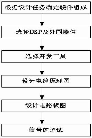
Figure 1 DSP intelligent controller hardware design flow chart
When selecting a device, consider the mutual matching between devices, as well as the availability and technical support of the device. The performance of the DSP chip TMS320F2812 selected in this design is as follows: high-performance static CMOS low-power design technology, the main frequency is up to 150MIPS (clock cycle 6.67ns), support JTAG boundary scan interface; high-efficiency 32-bit high-precision CPU; Up to 128K × 16 FLASH memory and so on.
The design of the circuit board requires knowledge of the transmission line theory and knowledge of the wiring process and system structure design to ensure signal integrity, and additionally consider electromagnetic interference and electromagnetic compatibility issues.
As shown in FIG. 2, the intelligent controller mainly comprises an analog circuit part (including a digital signal acquisition circuit and an output signal processing circuit), a DSP subsystem (including a DSP chip and a peripheral circuit), a power supply, a clock, and a reset circuit. The design of several major circuits will be described below.
Intelligent controller block diagram
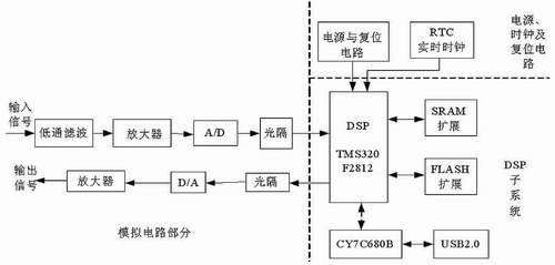
Figure 2 Intelligent controller block diagram
Power supply and reset circuit
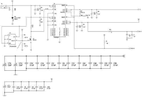
Figure 3 power supply and reset circuit
2 power supply and reset circuit design
The DSP system requires high performance of the power supply (such as ripple, power-on sequence, etc.), so the linear voltage regulator circuit chip TPS767D301 is selected in this design. The TPS767D301 is a dual output low leakage voltage regulator with the following features: Each power supply output has a separate reset and output enable control; it has a fast transient response function; the voltage output is adjustable from 3.3V/1.8V.
The power supply circuit composed of TPS767D301 introduces +5V voltage from the external regulated power supply, and the output voltage of the +5V voltage is 1.8V and 3.3V after TPS767D301. In order to reduce the interference of the power supply itself to the DSP, a filtering network is added in the circuit, as shown in FIG.
3 A / D, D / A circuit design
The TMS320F2812 has a 12-bit ADC with a 25MHz conversion frequency. The front end is two 8-to-1 multiplexers and two simultaneous samples/holders. When the requirements are not very high, it can be used to form a synchronous sequential sampling circuit, or an external sample holder can be added to form a synchronous sampling. Considering that the system has higher requirements on the accuracy and speed of power collection, the external six-channel 16-bit ADC ADS8364 is selected in the sampling module. The device includes six high-speed sample-and-hold amplifiers, six high-speed ADCs, one test voltage source, and three reference voltage buffers to provide a synchronous sampling rate of 250 KSPS and ultra-low power consumption (69 mW/channel) The conversion of all six input channels makes the unit cost of all channels low. The data output interface voltage of 6 channels is between 2.7 and 5.5V, which is convenient for direct interface with the DSP, eliminating the need for intermediate level shifting. Six fully independent ADCs greatly increase the overall parallel processing speed of the hardware, ensuring greater than 80dB of excellent common-mode rejection at 50kHz input signals, making them ideal for high-interference environments. Figure 4 shows the interface circuit between the ADS8364 and TMS320F2812.
In order to realize the control function of the system, the D/A converter circuit uses four 12-bit voltage output type DAC TLV5614, which has flexible four-wire serial interface, which can be seamlessly connected with TMS320 SPI, QSPI and Microwire serial port. The programming control of the TLV5614 consists of a 16-bit serial word, a two-bit DAC address, two independent DAC control bits, and a 12-bit DAC input value. The device operates from dual supplies: one for the digital interface used for the serial interface, DVDD and DGND, and the other for the analog supply used for the output buffer, AVDD and AGND. The two sets of power supplies are independent of each other and can be any value between 2.7 and 5.5V. The benefit of dual-supply applications is that the DAC operates from a 5V supply, while the digital portion of the DAC uses a 2.7-5.5V supply and can be connected to multiple interfaces.
Interface circuit of ADS8364 and TMS320F2812
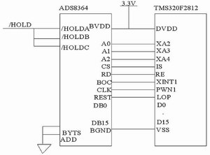
Figure 4 Interface circuit of ADS8364 and TMS320F2812
TLV5614 interface circuit
  
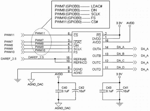
Figure 5 TLV5614 interface circuit
In the design, the D/A circuit uses a reference voltage of 2.5V. For control convenience, when controlling D/A, the GPIOB of TMS320F2812 is used as the conversion chip control line. The circuit is shown in Figure 5.
4 external SRAM, FLASH extended circuit design
Since the control system needs to store a large amount of data for analysis and utilization, according to the "zero wait" principle between the DSP and the external memory, the IS61LV6416-12T is used to extend the external memory of the F2812, and the IS61LV6416-12T is a 64K×16 high-speed CMOS SRAM. 3.3V power supply, its interface circuit with TMS320F2812 is shown in Figure 6.
External memory expansion circuit
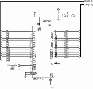
Figure 6 external memory expansion circuit
Design of Active Control Experimental System for Automobile Internal Noise
The control experiment system is mainly composed of four parts: the vehicle controlled system model (including the actuator), the external sound source, the controller and the signal monitoring (including the sensor), as shown in Fig. 7. It should be noted that in the control system, the controlled vehicle model contains a plurality of aluminum plates, and only one of them is drawn for convenience of expression.
In the experimental system, external speakers were used to simulate the excitation of the cabin from the outside. The sound waves emitted by the speaker force a surface of the automobile model to be forced to vibrate, causing large noise inside the car; when the sound pressure sensor placed at a specified position inside the box detects the sound pressure change there, The latest sound pressure value is transmitted to the DSP controller, and the controller makes a judgment according to the input and output conditions of the system at this time, and applies control to the system, and the control function is pasted on the thin aluminum plate wall of the closed cabin. The PZT actuator is completed because the PZT can generate vibration energy under the control signal, and the aluminum plate is also forced to vibrate, thereby reducing the noise at a specified position inside the car.
Experimental system composition diagram
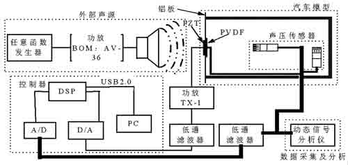
Figure 7 Schematic diagram of the experimental system
1 car controlled system model
Since this design is developed for the internal noise of the car, for the convenience of research, a rough car model is adopted as the controlled object. The four sides of the model consist of 1 mm aluminum plates with control sensors mounted on the body and inside the body. The actuator of the control system is PZT, which is mounted symmetrically on the model.
Since piezoelectric ceramics have the ability to convert electrical energy into mechanical energy, when the application system is energized to the piezoelectric ceramic, the spontaneous dipole moment of the material changes, thereby changing the size of the material, which can produce 50 μm in 20 ms. The displacement, the fast response speed is unmatched by other materials, and the frequency band is wide, it is not sensitive to temperature, and the performance tends to be stable with the increase of the number of pressurizations, and it is easy to integrate, which is necessary for high-precision, high-speed drives. material. This design uses the piezoelectric material PZT as the actuator.
2 external sound source
The external sound source in the experiment was replaced by a speaker, and the signal from the signal generator was driven by the power amplifier.
3 intelligent controller
The intelligent controller with TMS320F2812 DSP chip as the core can be operated independently offline and can be simulated online through USB interface.
4 signal monitor
In order to be able to monitor the control error signal and the piezoelectric chip drive signal in the box and perform signal processing, the signal monitor of the control system adopts a self-developed multi-function signal acquisition and processing system.
The piezoelectric material of the seat sensor selected for this design is the piezoelectric film PVDF, and the signal sensed by PVDF is used as the reference signal of the system. PVDF is thin, soft, low density and highly sensitive, and its mechanical flexibility is 10 times higher than that of piezoelectric ceramics. The piezoelectricity of the PVDF piezoelectric material is 3 to 5 times higher than that of quartz, and the piezoelectric coefficient is higher, and it can be attached to the surface of the object.
in conclusion
Based on TMS320F2812 DSP, this paper designs an intelligent controller that can run offline and independently and can be simulated online through USB interface. The vehicle internal noise active intelligent control experimental system is designed with the controller as the core. Through theoretical analysis, the control system has high data processing capability and processing speed, so it can play an important role in real-time control.
Table Top Stove,Single Burner Gas Cooker,Stainless Steel Portable Stove,Indoor Portable Gas Stoves
Xunda Science & Technology Group Co.ltd , http://www.xundatec.com