
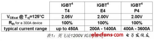
IGBT technology cannot fall behind application requirements. As a result, Infineon has introduced the latest generation of IGBT chips to meet the needs of specific applications. The switching speed and softness requirements associated with current inverter design application power or respective rated current levels are the main drivers driving these different types of device optimization. These models include the T4 chip with fast switching characteristics, the P4 chip with soft switching characteristics, and the E4 chip with switching speed between T4 and P4.
Table 1 briefly introduces the three trade-off points of the IGBT and gives recommendations for the corresponding current range.
Dynamic losses of IGBTs and diodes
To investigate and compare the switching losses and softness of these three different chips with stray inductance from 23nH to 100nH, we chose a module that is close to optimizing the reasonable limits of the T4 chip. Therefore, choose a common 62mm package 300A half-bridge configuration as the platform, and the module is equipped with these three IGBT chips.
All three modules use the same high-efficiency emitter control diode and gate drive settings. Figure 1 shows the experimental setup.

Figure 2 shows the effect of two different stray inductances on the turn-on waveform of a 300A half-bridge with IGBT-T4.

When the current rises, the higher stray inductance Ls can not only increase the inductor voltage drop of the device terminals (Δu=-L*di/dt), but also affect the current rise speed di/dt itself. Although the parasitic inductance slows down the conduction speed, the conduction loss is greatly reduced.
In this example, the loss in the initial switching phase (see timestamp a in Figure 2) decreases from 30.4 mW to 12 mW as the stray inductance increases.
The second phase of the switching event is characterized by a reverse recovery current peak in the diode and a further drop in the IGBT voltage. An increase in parasitic inductance results in a delay in the peak of the reverse recovery current and an increase in the switching loss in the second phase.
Therefore, for the entire switching event, an increase in parasitic inductance can significantly reduce the turn-on loss. In this example, the loss is reduced from 40mW to 23.2mW.
It is well known that although di/dt can reduce the voltage of the IGBT during the turn-on process, it also increases the voltage overshoot of the IGBT during the turn-off process. Therefore, an increase in the DC bus inductance increases the turn-off loss. As shown in Figure 3, the shutdown switch event can be divided into two phases.
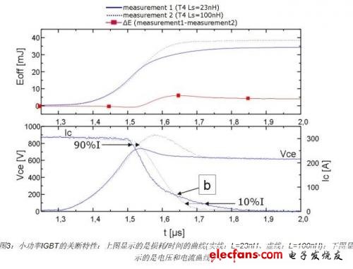
The current waveform set by the small inductor and the large inductor crosses at the position of the time stamp b. In the first switching phase up to the intersection b, the use of a large inductor to set the elevated overvoltage increases the loss to 36.3 mJ, while the small inductor sets the loss to 30.8 mJ. However, after point b, the large inductor setting produces a shorter current tail, so that the loss at this stage is 1.8mJ lower than the loss set by the small inductor. This result is mainly affected by the reduction in current tailing, which is a value that reaches 10% more quickly.
As the stray inductance increases, the turn-on loss of the IGBT decreases and the diode loss increases (as shown in Figure 4). Figure 4 shows a comparison of diode recovery characteristics for small inductors and large inductors.
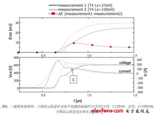
Obviously, the reduced di/dt of the IGBT has almost no effect on the loss at the beginning of the diode commutation because the diode voltage remains at around zero. After the peak current is reversed, the increase in diode voltage caused by the larger stray inductance determines and causes additional losses. The intersection point c can be seen again in the diode tail current set by the small inductance and the large inductance. A higher overpressure causes the loss before point c to increase from 10.1 mJ to 19.6 mJ. As in the case of IGBTs, the increased dynamic overvoltage causes the tail current to decrease after point c, and the loss balance of the large inductor setting is optimized to 4.4 mJ. In summary, the first switching phase plays a leading role, and the diode loss increases from 24.6 mJ to 29.7 mJ with an increase in inductance, an increase of 20%.

Although the combination of di/dt and parasitic inductance reduces the voltage of the IGBT during turn-on, it increases the voltage overshoot of the IGBT during the turn-off process. Comparing the turn-on and turn-off processes to the left and right, it is easy to see that the turn-off loss is much higher than the turn-off loss increase in the case of large parasitic inductance.
If we consider that the turn-off di/dt of the latest trench gate-off IGBT is essentially limited by the dynamic performance of the device, it is easy to understand this trend by about half of the conduction di/dt.
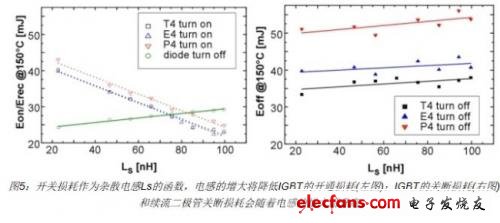
In Figure 5, the IGBT turn-on loss, turn-off loss, and diode commutation loss are compared to the parasitic DC bus stray inductance of the three IGBTs.
Softness and current abrupt characteristics of IGBTs and diodes
It has been shown previously that parasitic inductance may be beneficial for overall wear leveling. However, stray inductance can also cause oscillations, such as oscillations caused by sudden changes in current, which can result in limited device usage due to EMI or overvoltage limitations. All measurements described so far have been carried out at a junction temperature of Tvj = 150 °C, which is critical to the loss. The sudden change in current is more critical at low temperatures because the carrier injection of the device decreases with decreasing temperature and greatly reduces the charge used to smooth the tail current. Therefore, Figure 6 compares the IGBT turn-off of the three chips at rated current at 25 ° C and 600 V DC bus voltage. The DC bus inductance is used as a parameter.
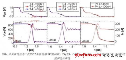
In the given example, when the stray inductance is about 55nH, T4 will harden and oscillation will begin to occur. Under the same conditions, E4 still maintains softness until the DC bus inductance reaches approximately 80nH. For the P4 chip optimized for high power, it remains soft within the observed inductance range (20nH...100nH). This observation is not surprising, as the IGBT is designed for high power modules up to 3600A rated current.
Although the sudden change in current of IGBTs is usually most noticeable at low temperatures and high currents, the softness of freewheeling diodes is usually the most critical at low temperatures and low currents. This depends on several factors: Because the diode is a carrier life-cycle optimization device, the plasma density is lowest at low currents, so the tail charge decreases as the current level decreases. In addition, switching IGBTs that force diode commutation typically switch faster at low current levels. Finally, the diode overvoltage is independent of the switching current, but is caused by the negative slope of the diode's reverse recovery current peak, which is also steepest at low currents and low temperatures.
Due to the effects of fast switching transients (du/dt and reverse recovery di/dt), DC bus oscillations can be easily triggered at low current levels, even without a sudden change in diode current. Figure 7 shows the reverse recovery characteristics of a freewheeling diode under different stray inductance conditions.

At this point, low stray inductance can provide a higher resonant frequency and help to suppress this oscillation. Of course, if the large stray inductance causes the diode to suddenly change in current, the situation will be even worse. This will limit the use of higher stray inductance due to EMI considerations.
Summary of this article
When operating under the same conditions, IGBT optimization for improved softness requirements will pay for the increase in switching losses.
In addition to switching losses, turn-on and turn-off speeds, sudden changes in current, and oscillations (EMI) are becoming more important. Parasitic stray inductance plays an important role in DC bus resonance frequency and diode current abrupt change. At least from an EMI perspective, a sudden change in diode current will limit the turn-on loss by increasing stray inductance or increasing the turn-on speed of the IGBT.
Therefore, it is expected to introduce different types of IGBT optimization products in the future. On the other hand, considering that the DC bus inductance is a free parameter in the inverter design, this will help to further optimize the losses.
Importantly, to ensure fast switching devices such as T4 chips, the DC bus design must be further optimized. In energy-efficient designs, the lower the better the inductor, the simpler principle.
Pad Mounted Transformer,Wind Power Substation,Step-Up Wind Power Sustation,Step Up Transformer
Hangzhou Qiantang River Electric Group Co., Ltd.(QRE) , https://www.qretransformer.com