
Abstract: The PL3105 chip is a special SoC chip designed for smart meters. It has powerful functions such as 8051 instruction-compatible high-speed microprocessors and direct sequence spread spectrum carrier communication. This article introduces the main features of PL3105 and its carrier communication principles, and analyzes software design methods for carrier communication applications.
introduction
With the rapid development of embedded system and integrated circuit technology, special chips designed for smart instrument applications have made great progress. Smart meters generally have CPU unit, display unit, standard industrial bus interface, A / D signal conversion, real clock, watchdog and other functions. After selecting the CPU, the traditional smart instrument equipment needs to configure complex function chips and interface chips to complete the display driver, external program storage, data storage and other required functions. Numerous interface chips lead to large volume, high cost, increased power consumption, and reduced reliability of the instrument; at the same time, debugging and maintenance are difficult.
In order to adapt to the application needs of smart meters, the dedicated single-chip system on chip (SoC) solution for certain products has gained huge development opportunities. IC design companies at home and abroad have launched their own SoC products for different fields and different application needs. The SoC product PL3105 with 8051 instruction compatible high-speed microprocessors is manufactured using the latest CMOS digital / analog hybrid process and is a low-cost, high-performance solution for smart meter industry applications. 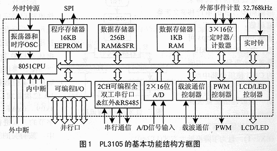
1 Main features of PL3105
Using 8051 instruction-compatible high-speed microprocessor, the software is easy to develop; with 8 / 16-bit dual-mode ALU, 8 times faster than the standard 51, fast operation speed, strong data processing ability. Figure 1 is a block diagram of the basic functional structure of PL3105.
For the application of smart meters, PL3105 integrates 2-channel 16-bit precision ∑-Δ modulation A / D, LED (8 & TImes; 8 strokes) / LCD (24 & TImes; 4 strokes) display drive module, 2 UARTs, built 1KB RAM and 16KB E2PROM program memory (programmed in ISP mode); built-in low-power real clock. At the same time, it integrates perfect voltage monitoring, power-on and power-off reset, and a watchdog circuit to ensure the reliability of the system when operating in an industrial environment.
The built-in carrier communication control unit makes the product have the powerful functions of networking and remote communication on the low-voltage power line; the upgrade of the lowest voltage power line carrier communication interface special chip PL2101, which has strong resistance to in-band co-channel interference and high sensitivity advantage. The embedded CPU realizes the control of the carrier communication through the configuration register, which is more convenient than the PL2101 chip interface and has higher reliability. 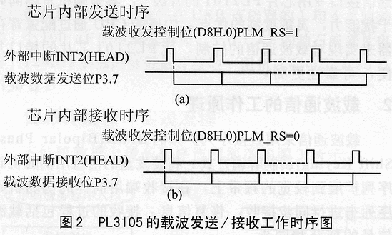
2 Working principle of carrier communication
Carrier communication adopts the BPSK (Bipolar Phase Shift Keying) modulation and demodulation method of direct sequence spread spectrum: the information to be transmitted is extended to a relatively higher frequency band with a pseudo random code sequence, and the same pseudo random code sequence is used for synchronization at the receiving end Receive and restore information. The receiving process includes carrier signal acquisition and synchronization.
Acquisition is that the receiving module searches the received signal before the spreading sequence is accurately synchronized, so that the phase of the received signal's spreading sequence and the local spreading sequence can be kept in synchronization, that is, the phase of the two is in a spreading sequence Within the symbol. Using a serial integral search method with a half-bit per step, the theoretical maximum acquisition time requires 29 data bits (at 15-bit PN code). After the acquisition is completed, it enters the tracking phase, and the clock rate of the local pseudocode generator is dynamically high-speed, so that the local pseudocode can automatically maintain accurate synchronization with the pseudocode of the received signal. The tracking circuit of the spread spectrum sequence uses an all-digital baseband delay locked loop (delay locked loop) circuit. 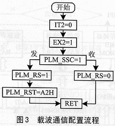
In order to ensure that both the acquisition and synchronization can be completed during the despreading process, the sending module sends at least 40 bits of all "1s" before each transmission of valid data, which is used for acquisition and ibid training (15 bit PN code).
Because the selected spreading pseudocode has strong autocorrelation, it is determined whether to stop the sliding of the pseudocode and complete the acquisition by comparing the correlation between the local pseudocode and the received sequence and the set threshold. At 500bps, the default capture threshold is 30H. Carrier communication's spreading and despreading work is completely realized by the hardware circuit inside the SoC, which is simple and reliable, and the despreading threshold can be adjusted by software.
Figure 2 (a), (b) is the timing diagram of the carrier communication transmission / reception operation within the PL3105. The transmit and receive data bits are connected to P3.7 inside the chip, and the chip is not packaged.
The carrier communication controller adopts serial shift communication in frame synchronization mode, half-duplex mode, and the rate is 500bps / 250bps; the center frequency is 120kHz, and the bandwidth is ± 7.5kHz. The built-in CPU uses external interrupt 2 (INT2), synchronous transceiver interrupt, carrier communication configuration process shown in Figure 3.
â‘ Enable INT2 interrupt (EX2 = 1), and it is the falling edge trigger mode (IT2 = 0).
â‘¡Enable carrier communication control bit PLM_SSC (EXT_CFG.0 = 1, INT2 as the interruption of carrier communication synchronization signal.
â‘¢ When the carrier transceiver control bit PLM_RS (EXT_CTRL.0) = 1, the carrier controller is in the sending state; when PLM_RS (EXT_CTRL.0) = 0, the carrier controller is in the receiving state.
â‘£Carrier transmission reset register: It is used to prevent the carrier communication module from being in the transmission state for a long time and set the entire communication system out of control. It is a 13-bit counter. In the transmission state, the counter decreases rapidly, and after decrementing to 0, the carrier transmission mode is forced to return to the receiving state; when receiving, the counter stops working. When sending data for a long time, it is necessary to write "A2H" to the PLM_RST register. After writing, the counter is automatically reset to keep sending.
The principle structure block diagram of low-voltage power line carrier communication is shown in Figure 4. It needs to cooperate with the peripheral power amplification and receiving loop. The distance of carrier communication is closely related to the advantages and disadvantages of peripheral circuit design and power. 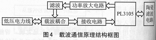
3 Software design for receiving and sending
Carrier communication is bus communication, so the normal state of the carrier module must be set to the receiving state, and different carrier modules must be assigned different communication addresses. After the module receives the correct command, only modules with the same address are allowed to respond according to the protocol. Because the carrier communication rate is much lower than the main frequency, in order to improve the efficiency of the CPU, the reception and transmission are generally designed as external interrupt processing; each time the interrupt is entered, the reception or transmission of 1 bit of data is completed.
After configuring the module according to the process shown in Figure 3 and selecting a rate of 500 bps, the internal selection is automatically a 15-bit PN code. The carrier communication controller enters the receiving state, and the carrier signal is captured and synchronized.
When receiving, the acquisition and synchronization process is automatically completed by the hardware circuit of the carrier communication control unit, without the need for software to participate. Since the cry of the power line has always existed, the synchronization frame header must be added before the valid data. According to the correlation standard, 0x09 and 0xAF are selected, followed by the valid data body and check byte of the communication.
Figure 5 is a block diagram of the carrier communication receiving process. After the carrier communication control unit despreads 1-bit data, an interrupt is generated. When receiving, first use the 16-bit receiving window and 1-bit sliding mode to receive the synchronization frame header 0x09 and 0xAF of the communication. After the frame header is successfully received, the subsequent data is intercepted in the manner of one byte per 8 bits to obtain valid data for transmission. During the reception process, address identification, length reception, and verification calculation are performed according to the relevant communication protocol. Modules with the same address respond to data that conforms to the communication protocol and transition to the sending state. 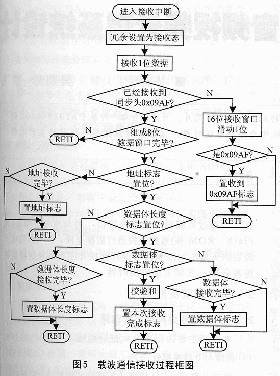
Figure 6 is a block diagram of the carrier communication transmission process. The calling party used for carrier communication issues a command or the receiving party's response. When set to the carrier transmission state, the carrier communication control unit sends a 1-bit spread spectrum data, and automatically generates an interrupt to allow the next data transmission. According to the needs of the capture and synchronization process, first send at least 40 bits of all "1"; then send the synchronization frame header 0x09, 0xAF bit by bit; then send the communication address, data length, data body, check bit by bit according to the user's relevant communication protocol Equal bytes.
After all the data is sent, the carrier module can be transferred to the receiving state. However, in order to ensure that the last bit of the data to be sent is successfully sent, it is necessary to wait for the next transmission interrupt after the last bit of data is sent before switching the carrier transmission state to the reception state.
The carrier has not been sent. Before sending all the data, the CPU must write "A2H" to the PLM_RST register in time to reset the counter and avoid automatic reset to enter the carrier receiving state in advance. The sending interrupt procedure is as follows:
void PLM_int (void) interrupt 7 // Carrier transceiver interrupt
{if (PLM_RS == 1) zb_tx (); // Carrier transmission interrupt service program
else zb_rx (); // Carrier receiving program service program, omitted
}
void zb_tx (void) // carrier transmission procedure
{if (len8 == 0) s_byte = buf_send [zbs_count]; // Fetch the bytes to be sent to send buffer in place 
ACC = s_byte;
P3.7 = ACC ^ 7; // Bit transmission, the highest bit is first
s_byte = s_byte << 1; // left shift
len8 ++; // shift count calculation
if (len8> 7) // 8 bits are sent
{zbs_count ++; // Next byte
len8 = 0; // Clear shift count
}
PLM_RS = 1; // Allow carrier transmission
PLM_RST = 0xA2; // The carrier transmission reset register is cleared
}
Conclusion
The smart meter with carrier communication function designed by the SoC chip PL3105 has been applied and popularized in the smart meter industry. Its simple receiving and transmitting processing methods make application design very convenient. At the same time, the flexible ISP programming method makes the product upgrade and function expansion flexible; it reaches the low-cost and high-performance design index.
Liquid Crystal Display For Medical Use
Liquid Crystal Display For Medical Use,Super Liquid Crystal Instrument Medical Display,Medical Liquid Crystal Instrument Lcd Display,Thin Transparent Lcd Medical Display
Dongguan Yijia Optoelectronics Co., Ltd. , https://www.everbestlcdlcm.com