
When an external overvoltage condition occurs in the amplifier, the ESD diode is the last line of defense between the amplifier and the overvoltage. A proper understanding of how the ESD unit is implemented in a single device allows the designer to greatly extend the amplifier's lifetime through proper circuit design. This article is intended to introduce the reader to various types of ESD implementations, discuss the features of each, and provide guidance on how to use these units to improve design robustness.
introduction
There are many applications where input is not controlled by the system, but is connected to the outside world, such as test equipment, instrumentation, and some inspection equipment. For such applications, the input voltage may exceed the rated maximum voltage of the front-end amplifier, so a protection scheme must be used to maintain the design's range of use and robustness. The internal ESD diode of the front-end amplifier is sometimes used to clamp over-voltage conditions, but there are many factors to consider in order to ensure that this clamp provides adequate and reliable protection. Understanding the different ESD diode architectures inside the front-end amplifiers, as well as the thermal and electromigration effects of specific protection circuits, helps designers solve protection circuit-related problems and increase their lifetime in the field.
ESD diode configuration
It should be understood that not all ESD diodes are simple diode clamps connected to the power supply and ground. There are many possible solutions, such as multiple diodes in series, diodes and resistors, back-to-back diodes, and so on. Here are some of the more common scenarios.
Diode connected to the power supply
Figure 1 shows an example of an amplifier with a diode connected between the input pin and the power supply. Under normal operating conditions, the diode is reverse biased, but when the input is above the positive supply voltage or below the negative supply voltage, the diode becomes forward biased. When the diode becomes forward biased, current flows through the input of the amplifier to the corresponding supply.
For the circuit shown in Figure 1, when the overvoltage exceeds +Vs, the amplifier itself does not limit the input current, and external series resistors are required to limit the current. When the voltage is lower than –Vs, the 400 Ω resistor will have a certain current limiting effect and should be considered in the design.
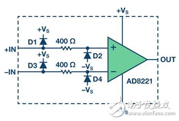
Figure 1. Input ESD topology for the AD8221
Figure 2 shows an amplifier with a similar diode configuration, but in this case, the current is limited by the internal 2.2 kΩ series resistor. It differs from the circuit shown in Figure 1 not only in the value of the current-limiting resistor R, but also in that 2.2 kΩ protects the circuit from voltages above +Vs. This example is complicated and difficult to understand, so be sure to fully understand it to optimize protection when using ESD diodes.
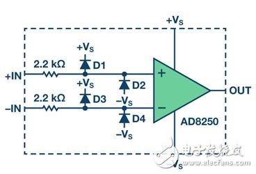
Figure 2. Input ESD topology of the AD8250
Zhejiang Baishili Battery Technology Service Co,.Ltd. , https://www.bslbatteryservice.com