
Center topic:
This article refers to the address: http://
Four different loads in a load-controlled pre-FET driver and N-channel power FET combination control system
Set the dynamic fault threshold for inrush current
Fault detection and protection of vehicle lighting systems
solution:
Combine a high-voltage side pre-FET driver with a power FET to control automotive lighting
Electronic switches are programmed to perform periodic automatic retries in the event of an overcurrent condition
Combination of pre-FET driver and power FET prevents dynamic and static faults in the application
FET protection by recirculating solenoid energy and installing a rectifier in the load
On-board lighting systems require peak surge currents of up to 55A. In conventional methods, the use of relays and fuses to switch and limit the power output current is unpredictable and unreliable.
Combining a high side pre-FET driver with a power FET is an ideal solution for controlling automotive lighting.
The resistance of a tungsten wire in an incandescent bulb can vary over a 1:10 ratio as a function of temperature. An electronic switch with programmable short-circuit and over-current regulation is extremely useful to prevent component overheating and component degradation due to prolonged use. Once an overcurrent condition is detected, the standard and self-recovery (re-settable) fuses interrupt the load supply and may take a length of time to reset. In contrast, an electronic switch can be programmed to react more predictably.
Fuse-based systems can only be set to a definite reset value and cannot accommodate a 10:1 current ratio like an electronic solution. The electronic switch can be programmed to perform periodic automatic retries in the event of an overcurrent condition or to check if the fault has been eliminated. At the same time, monitoring, detecting, and reporting the nature of the fault helps to easily identify the system's problems.
The multi-channel pre-FET driver and external power FET concept provides system flexibility to optimize load control power and cost. Independently selecting power consumption and different FET resistances helps prevent interactions and system failures due to single-channel faults compared to a fully integrated solution.
The combination of the pre-FET driver power switch allows the system to control the FET switching characteristics and handle all electromagnetic interference (EMI) issues when using external RC components on the gate drive output.
Load-controlled pre-FET driver and N-channel power FET combination
A pre-FET driver (eg, the TPIC44H01 from TI) is used to control four different loads in the system. This combination enables better control of the resistive load by the temperature coefficient. Typically, the load is connected to the low side and the power FET is configured on the high side to power the load. Each channel can be controlled by a parallel input signal from the microcontroller or a serial programming register. In a parallel architecture, a general purpose I/O or timer based output is used to control the load current.
The gate drive output is typically a constant current source and sinks the output to control the FET gate capacitance charge and discharge characteristics. An external resistor in series with the output limits the number of FET switch transitions. This effect allows the slew rate to be controlled while also helping to reduce the rapid current changes that occur during switching limits that increase electromagnetic interference (increasing switching losses and power dissipation). These outputs are internally controlled below the maximum output voltage of 17V to protect the external FET gate from source breakdown damage. The combination of the pre-FET driver and power FET can be configured to prevent dynamic and static faults in the application compared to an integrated solution.
Dynamic fault threshold for inrush current
Luminous illumination of incandescent lamps requires a dynamic fault threshold to compensate for high inrush currents and to prevent erroneous triggering of overcurrent conditions at the beginning of the opening. The use of a RC network with a switch sets the threshold for this dynamic fault (see Figure 1). By using this method, the short-circuit current can be optimized for different incandescent bulbs. The VPEAK voltage is set when the initial overcurrent threshold is set and then attenuated when the resistor divider value set on the VCOMP terminal is a constant RC time constant. This variable overcurrent threshold waveform is generated by a parallel or serial input bit of an appropriate channel each time the gate transitions from the "off" state to the "on" state.
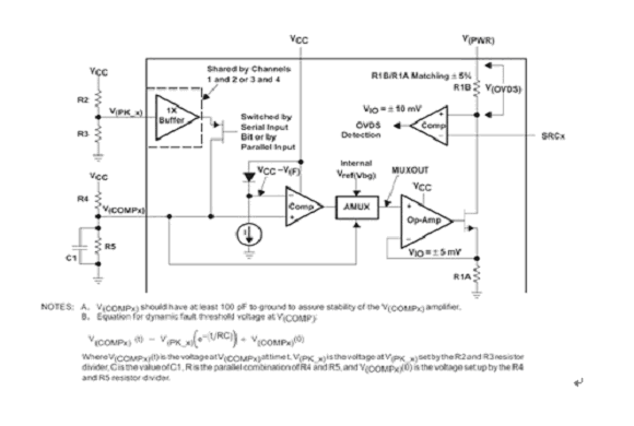
figure 1
The programmed VPEAK(X) value is reflected on VCOMP(X) when the particular channel is in the "off" state. If a particular channel is turned on, the reference voltage for overcurrent detection is dynamic and is represented by the internal VPEAK setting and the VCOMP(X) terminal external component value.
An overcurrent fault threshold, expressed in voltage form, is adjusted based on time to compensate for changes in the filament filament resistance (as shown in Figure 2).
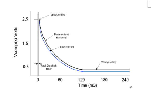
figure 2
Fault detection and protection
In all systems, fault detection is critical for load protection. The ability to independently detect faults in the "on" state for short-circuit loads and overcurrents, as well as for each channel with an open load in the "off" state, will enable the system to react correctly. This type of detection also isolates faulty channels to avoid affecting other normal channels, especially when it comes to thermal interaction problems.
a “on†status failure
To detect the short-circuit load on each channel, monitoring the external power FET supply voltage ensures that the switch is fully "on" and when the voltage is set to several positive voltages (typically 5V). If the short-circuit load occurs after the switching transition, the fault is determined to last longer than the fault mask time before the system responds correctly (including "turning off" the FET so that it does not exceed the safe operating area parameters). To prevent false fault reporting during switching transitions, an anti-glitch filter is activated to de-energize the transition time to mask the fault. The anti-spike masking time can be programmed to compensate for all slew rate control implementations.
Overcurrent fault monitoring and reporting is flagged when the drain-to-source voltage on an external pin exceeds a programmed voltage level. This approach requires the FET resistor to be in the "on" state and requires all load currents to generate the drain-source voltage. Detection of such faults is masked during programming called a fault mask timer. If the fault persists for a longer period of time than the mask timer, an overcurrent fault will be reported and the correct action is taken to "turn off" the FET. This arrangement prevents the FET from exceeding the device's highest recommended junction temperature.
When an overcurrent condition is detected, the FET can be protected by "turning off" the device or activating an option setting that will automatically retry and "turn on" the FET with a low duty cycle. This allows the system to constantly check to see if the fault has been eliminated and will not destroy the FET. Figure 3 shows the schematic of this overcurrent detection protection.
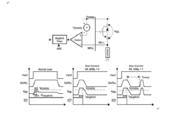
image 3
b "off" status failure
Monitoring open circuit load faults in the "off" state provides load integrity information to the system. By monitoring the supply voltage of the external power FET when the switch is fully "off", the detection of an open circuit load fault for each channel can be achieved. An internal power supply activates a small constant current flowing through the load to ground and biases the SRCx node below the open load detection threshold.
If an open load or high impedance is detected, a small constant current will bias the SRCx node above the open load detection threshold to detect the fault (see Figure 4).
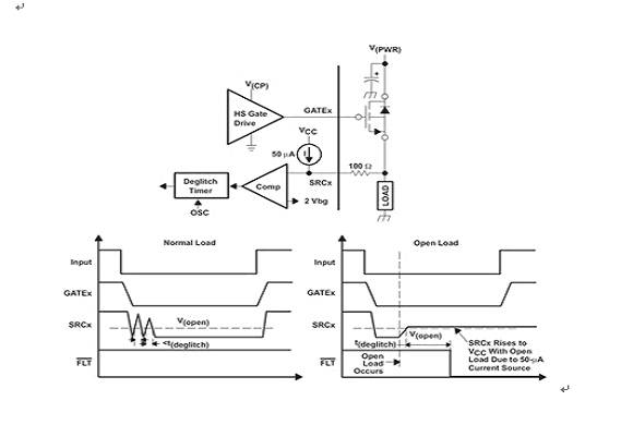
Figure 4
Similarly, to prevent erroneous fault reporting during switching, an anti-spike filter is activated during power conversion to mask the fault. The anti-spike masking time can be programmed to compensate for all slew rate control implementations. If the open load occurs after switching, the fault is determined to be valid longer than the fault mask before the system makes the correct action. The correct action is to keep the FET in the "off" state.
In all systems, it is important to monitor the overvoltage condition of the power line and “turn off†the FET to prevent possible damage to the load and FET (see Figure 5).
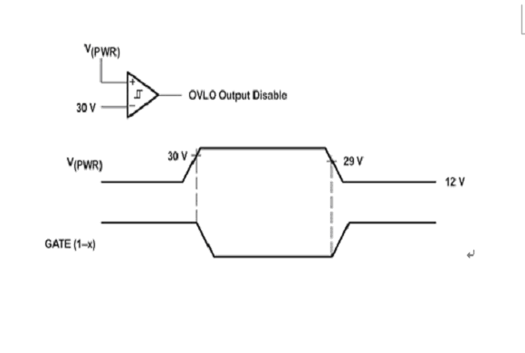
Figure 5
A combination of a pre-FET driver and a power FET can be used to drive the solenoid load. Damage to the power FET can occur if external protection is not implemented with the gate "off". The FET can be protected by recirculating the solenoid energy and installing a rectifier in the load. However, doing so may take some time to attenuate the load energy, so this method is not recommended for fast pulse width modulation (PWM) operation.
For a fast "off", "active" "on" power FETs requires an active clamp. This consumes the stored energy and quickly adds several watts of power to the FET in less than a millisecond. Alternatively, the avalanche breakdown of the external power FET can be used to slowly consume energy after "off", but this method is not recommended for high frequency pulse width modulation (PWM) operation.
in conclusion
High-voltage side pre-field FET drivers and power FET combinations are widely used for load control, such as incandescent bulbs for automotive electronics, relay solenoids, and transmission solenoids. This combination may also be used in industrial and commercial applications that require load control through serial bus communication or parallel input control. The ability to isolate each power FET from thermal interaction is very beneficial in situations where single-channel shorts or thermal shutdown faults do not interrupt other load control channel functions.
This Solder Wire is with activated resin flux,It enjoys excellent weld ability,which can be divided into RA and RMA.which is made from extremely high purity raw materials.
Sn63/Pb37,Sn60/Pb40,Sn50/Pb50,Sn45/Pb55,Sn40/Pb60,Sn30/Pb70
Flux-Cored Solder Wire,Solder Welding Wire,Lead Free Solder Wire,Silver Solder Wire
Shaoxing Tianlong Tin Materials Co.,Ltd. , https://www.tianlongspray.com