
The conditional access system (CAS) of digital TV is a part for program authorization and management of digital TV users, and is one of the important components in digital TV broadcasting. Among them, the use of open machine-card separation structure is an important future development trend of conditional access system. The separation of machine card is to separate a universal TV reception system suitable for mass production from a private CAS management system by defining a universal physical interface and related interface communication protocol on the user receiving terminal. At present, the implementation method of the machine-card separation mode in the world is to use a physical interface similar to the PCMCIA socket on the portable computer. The standard issued by the European DVB organization is called DVB-CI, and the United States has a similar standard called POD. In fact, the new PCMCIA standard document already includes the definition of these two interfaces. The PCMCIA card loaded with conditional access processing content is simply referred to as a digital TV conditional access card, and may be referred to as a CAM (conditional access module).
In fact, the establishment of the separation standard of the machine card, after opening a standard socket on the TV, its significance is not only to solve the problems of public viewing and private management, but its huge significance will also be reflected in the number as a household consumer product TVs have a way to upgrade performance and expand functions. Just like the current development scale of PC, it has an inseparable relationship with the standardization of PC's ISA, PCI, APG and other interfaces. We can hardly imagine whether the industry can achieve such great success if the computer does not have a standardized and extensible interface. In the field of digital TV, the establishment of a separate interface standard for machine cards and the opening of the standard interface on digital TV sets will introduce digital TV into a colorful development field. For example: for different program signal transmission methods (wireless broadcasting, cable, satellite, digital audio broadcasting), you can insert different types of receiving modules on the CI interface (machine card separation general interface); for our digital The photos stored on the camera memory card can be browsed on the TV through a universal memory card reader module; through the broadband IP receiving module, you can enjoy all kinds of streaming programs on the TV and two-way transmission on the network; you can pass through the gateway The module connects the TV and other electrical equipment into a home digital network system; with a hard disk recording module, users can record licensed programs and so on. In the future, its development trend and potential are more difficult to predict.
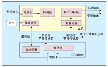
Figure 1: Schematic diagram of machine-card separation structure.
The structure of CAM can generally be based on a high-performance 32-bit SoC chip, with smart card interface, CI interface, dedicated TS transport stream processing engine, DVB general descrambling and other components. The volume of the CAM card is very limited, but it is necessary to realize a high-speed 32-bit embedded system that can handle high-definition TV program streams, so the size and performance of its core SoC chip has become a key point.
Through intensive research on the European DVB-CI standard, combined with our own product development experience in the field of embedded products and integrated circuits, we have tackled the problem of SoC technology with ARM7TDMI as the core, and successfully developed performance and integration in The world's leading CAM chip SM1658, while greatly reducing the production cost of CAM, eliminates the price bottleneck of large-scale promotion of machine card separation standards.
CAM structure and hardware system
SM1658 is a typical dedicated embedded microprocessor for CAM system. It integrates all the main functional modules of a CAM. The CAM structure with it as the core is very simple.
SM1658 uses the widely popular 32-bit ARM7TDMI as the CPU core. In addition to integrating common circuit modules such as memory management, interrupt controller, timer, watchdog, asynchronous serial communication, PLL and other common SoC chips, it is also internal It integrates 256KB high-speed SRAM, smart card interface, PCMCIA (DVB-CI) interface, high-speed TS stream demultiplexing / filtering engine and DVB general descrambler and other modules. Its basic structure is shown in Figure 1. Only a piece of external FLASH program memory chip is needed to form a high-performance CAM card.
The memory management module of SM1658 can support a total of 4 memory segments. This memory part can be internal or external SRAM or external FLASH. The data line width and read / write speed of each memory can be initialized and configured by software. The maximum capacity of each memory segment can support up to 4M bytes, and the four memory segments can support up to 16M bytes. Among them, the memory implemented inside the chip is a 256KB high-speed internal SRAM, which can execute the core program of the system at a high speed without waiting for a cycle, greatly improving the processing capacity of the chip's key programs.
SM1658's interrupt controller can provide 32-channel interrupt management. Each interrupt can choose priority level, trigger up / down edge, pulse / level trigger selection, and provides rich interrupt management features such as interrupt mask, interrupt reservation, and soft trigger. The CI physical interface is a subset of the PCMCIA standard. Can be divided into TS flow channel and command channel. Our CI interface fully conforms to the DVB-CI interface standard, and provides two-way buffer, CIS memory and flexible status and control registers on the hardware structure.
Three 16-bit timers are also provided inside the chip, each with an optional 8-bit prescaler. The watchdog of the chip is 32-bit. If the watchdog is not needed, it can be configured as a 32-bit timer.
design feature
1. Simple and efficient local bus
In SoC design, the choice of internal and external buses is a very important factor. An efficient and simple bus can improve the operating efficiency and scalability of the chip.
In the SoC chip design of the ARM architecture, ARM generally recommends using the standard AMBA bus for design. At the same time, the ARM7TDMI core itself also has a simple internal bus. Before deciding to adopt the bus specification, we conducted the following analysis on the architecture and application characteristics of SM1658.
One of the advantages of the AMBA bus is that it can support multiple master device calls, adjudication, and data pipeline processing. In SM1658, there is only one master device ARM7TDMI, the other module circuits are in the slave device state, and the CPU performs unified scheduling, and all external slave devices use the same clock as the master device, which can immediately respond to CPU access within a single clock . Therefore, it is more advantageous to use ARM7 local bus in this aspect.
If you use the AMBA bus, the design team can use a large number of third-party IP modules, these IP modules are in line with the AMBA bus specifications, and have undergone strict verification. In the chip design of SM1658, in order to reduce the cost of the chip to the greatest extent, at the same time, because the important module circuits are not suitable for IP, we have designed all the circuit modules ourselves. Then, the development time saved by using IP is not feasible.
In addition, if you use the AMBA bus, you must add a first-stage pipeline to the original three-stage pipeline of ARM7TDMI, and convert the bus structure of the dual-clock edge of ARM7TDMI to a single-clock edge bus structure, which can simplify the later design of the chip the amount. However, in this way, an extra clock cycle is lost for certain jump instructions, which reduces the working efficiency of the CPU. In addition, using the AMBA bus, the CPU and each module need to increase the interface logic of the AMBA bus, increasing the size and cost of the chip.

Figure 2: The basic structure of SM1658.
Finally, we decided to use ARM7TDMI's own local bus from the aspect of maximum use efficiency of the chip and simplified logic control. Using the local bus of ARM7 has several advantages: the local bus status of ARM7 is relatively simple, and no relatively complicated AMBA bus protocol verification is required; the interface function requirements of the module are low, and the interface circuit is very simple; the length of the pipeline is reduced to a maximum In the SoC chip whose clock is fixed by the IP hard core, the reduced pipeline means that the code execution efficiency of the chip is improved. At the same time, the strict constraint and verification of the double-edge clock problem on the ARM7 bus ensure the correctness of the later design of the chip.
2. Internal SRAM with software redundancy
ARM7TDMI is a CPU core without internal cache, and can only wait idle for slow SRAM and FLASH memory. Even if a high-speed external SRAM is used, the full performance of the high-speed CPU cannot be effectively used due to the width of the data interface and the data transmission delay between the chips; at the same time, the high-capacity high-speed SRAM is expensive and will be greatly increased The cost of the CAM system. Considering the system structure and cost, we decided to embed a 256KB SRAM in the SM1658. This SRAM capacity can meet the application requirements of quite a few CAM systems. At the same time, our chip also supports a variety of external high-speed and low-speed SRAM, which can meet the requirements of some systems with very high SRAM requirements.
The SRAM implemented inside the SM1658 has very high performance, and can complete the operation of various ARM instructions in a single clock cycle, that is, when the CPU fetches instructions or accesses data in the internal SRAM, there is no need to wait. After the chip was produced, we benchmarked the CPU performance with the SRAM inside the chip. Even at very high frequencies, the chip can obtain the same level as the theoretical calculation value of the ARM7TDMI IP core, and the test data is behind. form.
The biggest problem with embedded SRAM is that it has an impact on chip yield. We have taken some effective precautions in circuit function design, underlying software design, and application systems to greatly reduce the system's dependence on defective SRAM. In this way, the chip yield can be greatly improved. This also reduces the overall cost of the chip from a system perspective.
3. Clock circuit with dynamic adjustment
In the clock design of the SM1658 chip, we also integrated a software-configurable clock management circuit, called a dynamic clock circuit. We program the clock processing module of the chip through software, which not only allows the working clock frequency of the chip to change continuously as needed, to reduce the power consumption of the chip under light task load, but also can adapt to the input of multiple external clock sources and increase CAM The adaptability of the system in product development.
The Touch Monitor is a product developed and designed by ourselves. It has been sold for more than 6 years and has exceeded 160,000 units. At present, it is running very well. It mainly customizes different touch technologies, different sizes, different interfaces, connecting cables and power supply parts to meet the needs of guests. We provide customers with the choice of Resistive Touch Screen, Capacitive Touch Screen, Infrared Touch Screen and nano touch foil, and customize various interfaces for customers, such as: VGA, DVI, HDMI, DP and so on. It is mainly used in banks, hospitals, government units, airports, railway stations, supermarkets, real estate and other places.
Product show:
Touch Monitor
Touch Monitor,Wall Hang Touch Monitor,Vertical Floor Monitor,Dust-Proof Water Proof Touch Monitor
ShenZhen GreenTouch Technology Co.,Ltd , https://www.bbstouch.com