
Abstract: This application note explains how to configure the clock rate adapter (CLAD) in DS325X, DS316X, DS317X, and DS318X devices to generate multiple clock sources. In specific applications, these clock sources can be used as the LIU reference clock or transmit clock.
Introduction This application note explains how to configure a clock rate adapter (CLAD) to generate multiple clock sources. These clock sources can be used as the LIU reference clock or transmit clock by DS325X, DS316X, DS317X, and DS318X devices.
This application note applies to the following products.
Use the clock rate adapter unit inside the CLADDS325X T3 / E3 LIU in the DS325X to generate all required clock rates from a single input clock. If there is a transmission quality clock source (DS3, E3 or STS-1), the clock rate adapter can synthesize two other line rate transmission quality clocks. In this way, both the input clock and the synthesized clock can be used as the master clock for the clock and data recovery (CDR) unit and jitter suppressor. Driven by the LIU master clock, the CDR unit obtains the amplified and equalized signal from the AGC / equalizer unit, generating separate clock, data positive and data negative signals. In hardware mode, the clock rate adapter is completely controlled by the T3MCLK, E3MCLK, and STMCLK pins.
In the CPU bus mode, more control of the clock rate adapter can be provided through the CACR register. When the “AMCEN—Alternate Master Clock Enable†control bit is set to 1, the clock rate adapter is configured for the backup master clock mode. In this mode, the clock rate adapter no longer works on the DS3, E3, or STS-1 clock, but on a clock whose frequency is determined by the "Backup Master Clock Selection" (AMCSEL) control bit. As a backup master clock, the effective input frequencies are 19.44MHz, 38.88MHz and 77.76MHz. In the backup master clock mode, the clock rate adapter can synthesize up to two of the three clock rates (DS3, E3, or STS-1). To synthesize the DS3 and E3 clocks, the backup master clock can be connected to the STMCLK pin. To synthesize the DS3 and STS-1 clocks, you can connect the clock to the E3MCLK pin, and the clock to the T3MCLK pin can synthesize the E3 and STS-1 clocks.
Although the power-on default values ​​for AMCEN and AMCSEL [1: 0] in DS325X devices may not match the actual applied clock, a backup clock can still be applied to any MCLK pin at the beginning of power-up. Once these control bits are correctly configured after power-up, the clock rate adapter starts synthesizing the correct master clock. The entire device can work normally.
CPU bus mode can also output a synthesized master clock on the T3MCLK, E3MCLK, and STMCLK pins for use by neighboring framers, mappers, and other components. To output the synthesized DS3 master clock on T3MCLK, simply set CACR: T3MOE = 1. To output the synthesized E3 master clock on E3MCLK, set CACR: E3MOE = 1, or set CACR: STMOE = 1, and output the synthesized STS-1 master clock on STMCLK.
The DS325X CLAD configuration register is used to configure the CLAD clock rate adapter control register as described below.
Register name: CACR
Register description: Clock rate adapter control register register address: 08h
Bit 7: T3MCLK output enable (T3MOE). When the clock rate adapter is configured to synthesize the DS3 master clock, by setting T3MOE = 1, the DS3 master clock can be output on the T3MCLK pin. This clock can be used as a transmit clock for neighboring DS3 framers and other components that require a DS3 clock. This bit can be set to 1 only when the T3MCLK pin is not driven externally.
0 = T3MCLK output drive is disabled
1 = T3MCLK output drive is enabled
Bit 6: E3MCLK output enable (E3MOE). When the clock rate adapter is configured to synthesize the E3 master clock, the E3 master clock can be output on the E3MCLK pin by setting E3MOE = 1. This clock can be used as a transmit clock for neighboring E3 framers and other components that require an E3 clock. This bit can be set to 1 only when the E3MCLK pin is not driven externally.
0 = E3MCLK output drive is disabled
1 = E3MCLK output drive is enabled
Bit 5: STMCLK output enable (STMOE). When the clock rate adapter is configured to synthesize the STS-1 master clock, the STS-1 master clock can be output on the STMCLK pin by setting STMOE = 1. This clock can be used as a transmit clock for neighboring SONET framers, mappers, and other components that require an STS-1 clock. This bit can be set to 1 only when the STMCLK pin is not driven externally.
0 = STMCLK output drive is disabled
1 = STMCLK output drive is enabled
Bit 2 to Bit 1: Backup master clock selection (AMCSEL [1: 0]).
00 = 19.44MHz
01 = 38.88MHz
10 = 77.76MHz
11 = not defined
Bit 0: Backup master clock enable (AMCEN).
0 = Disable backup master clock mode
1 = Enable backup master clock mode
Use CLADDS316X in DS316X, DS317X, and DS318X, CLAD in DS317X, and DS318X to generate multiple internal clock frequencies (DS3, E3, or STS-1) from a single reference clock input from the CLKA pin. The clock frequency of input CLKA must be one of the following: DS3 (44.736MHz) E3 (34.368MHz) STS-1 (51.84MHz) If one of the above clocks is provided, the other two can be generated. If necessary, these internal clocks can drive the output pins CLKB and CLKC for external use.
CLAD with DS316X, DS317X and DS318X
If you use the DS317X or DS318X LIU, CLAD can provide a clock to the DS317X or DS318X receiving LIU. The CLAD of DS316X, DS317X and DS318X is configured by the CLAD bit in the GL.CR2 register.
In this case, the user must provide the DS3, E3, or STS-1 clock on the CLKA pin. The user must provide at least one of the three frequencies (DS3, E3, or STS-1) to the CLKA pin. The CLAD [3: 0] bits inform the PLL what frequency is applied to these pins. Figure 1 shows the CLAD units of DS316X, DS317X and DS318X.
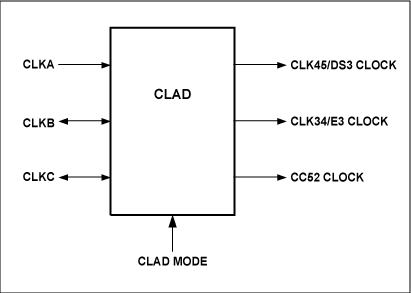
Fig. 1. CL316 unit of DS316X, DS317X and DS318X
The FM bit (located in PORT.CR2) is used to select the clock output by CLAD and applied to LIU and the transmitter. CLAD has high flexibility. You can accept any of the three clock frequencies and use CLAD to provide the remaining required frequencies.
CLAD can also be disabled, all three clocks are provided externally, using the CLKA, CLKB, and CLKC pins as inputs. When CLAD is disabled, the three reference frequencies DS3, E3, and STS-1 must be applied to the CLKA, CLKB, and CLKC pins, respectively. If some of the three frequencies are not used, it is not necessary to apply this frequency on the corresponding CLAD clock pin.
The CLAD [3: 0] control bits (located in the GL.CR2 register) control the working mode of CLAD, which determines the input and output characteristics of each pin and the clock frequency corresponding to each pin. Please refer to Table 1 below for details.
When CLAD [3: 0] = 00XX, the PLL circuit is disabled, and the input clocks on the CLKA, CLKB, and CLKC pins are used as the reference clock for the internal LIU. When CLAD [3: 0] = (01XX or 10XX or 11XX), there will be zero, one or two PLL circuits enabled to generate the required clock, depending on the CLAD [3: 0] bits, frame mode (FM [5: 0]) bits and the line mode control bits (LM [2: 0]) in PORT.CR2.
The line mode bit selects the working mode of the master port. If there is no need to generate a clock to output through the CLAD output pin or as the reference clock for LIU, then the corresponding PLL used to generate the clock is disabled and is in a power-down state.
The CLAD configuration registers of DS316X, DS317X and DS318X are used to configure the two registers of CLAD as shown below.
Register name: GL.CR2
Register description: Global Control Register 2
Register address: 004h
Bit 3 to 0: CLAD input / output mode [3: 0] (CLAD [3: 0]). These bits are used to control the clock input / output pins CLKA, CLKB, and CLKC of CLAD. These register bits determine which clock is used to recover the Rx clock from the LIU line. Table 1 lists the details.
Table 1. CLAD input / output pin coding details
CLAD provides a reference clock for receiving LIU. The receiving LIU selects the clock frequency according to the mode selected by the user (via the frame mode (FM) bit). The FM bit selects the main framing operating mode. If selected by the PORT.CR3.CLADC register bits, the CLAD output can also be used as the transmit clock source.
Register name: PORT.CR3
Register description: Port Control Register 3
Register address: (0, 2, 4, 6) 44h
Bit 3: CLAD transmit clock source control (CLADC). This bit is used to select the CLAD clock as the internal transmit clock source. The function of this bit is related to the setting of other control bits.
0 = CLAD clock is allowed to be used as transmit clock.
1 = The CLAD clock is not used as the transmit clock (if the loopback function is not enabled, the clock source is TCLKIn).
Conclusion DS325X, DS316X, DS317X, and DS318X devices include a CLAD function that can be used to generate a variety of clocks as a LIU reference clock, or for user applications as a transmit clock. If you have further questions about the work of CLAD in Maxim devices, you can email var name = "telecom.support @"; var domain = "maxim-ic.com"; document.write ("" + name + domain + " "); telecom. (English only) or call USA 972-371-6555 (English only) to contact Maxim's telecom application support team.
Introduction This application note explains how to configure a clock rate adapter (CLAD) to generate multiple clock sources. These clock sources can be used as the LIU reference clock or transmit clock by DS325X, DS316X, DS317X, and DS318X devices.
This application note applies to the following products.
| T3 / E3 LIUs | T3 / E3 ATM / Packet PHYs | T3 / E3 SCTs | T3 / E3 ATM / Packet PHYs with LIUs |
| DS3251 | DS3161 | DS3171 | DS3181 |
| DS3252 | DS3162 | DS3172 | DS3182 |
| DS3253 | DS3163 | DS3173 | DS3183 |
| DS3254 | DS3164 | DS3174 | DS3184 |
Use the clock rate adapter unit inside the CLADDS325X T3 / E3 LIU in the DS325X to generate all required clock rates from a single input clock. If there is a transmission quality clock source (DS3, E3 or STS-1), the clock rate adapter can synthesize two other line rate transmission quality clocks. In this way, both the input clock and the synthesized clock can be used as the master clock for the clock and data recovery (CDR) unit and jitter suppressor. Driven by the LIU master clock, the CDR unit obtains the amplified and equalized signal from the AGC / equalizer unit, generating separate clock, data positive and data negative signals. In hardware mode, the clock rate adapter is completely controlled by the T3MCLK, E3MCLK, and STMCLK pins.
In the CPU bus mode, more control of the clock rate adapter can be provided through the CACR register. When the “AMCEN—Alternate Master Clock Enable†control bit is set to 1, the clock rate adapter is configured for the backup master clock mode. In this mode, the clock rate adapter no longer works on the DS3, E3, or STS-1 clock, but on a clock whose frequency is determined by the "Backup Master Clock Selection" (AMCSEL) control bit. As a backup master clock, the effective input frequencies are 19.44MHz, 38.88MHz and 77.76MHz. In the backup master clock mode, the clock rate adapter can synthesize up to two of the three clock rates (DS3, E3, or STS-1). To synthesize the DS3 and E3 clocks, the backup master clock can be connected to the STMCLK pin. To synthesize the DS3 and STS-1 clocks, you can connect the clock to the E3MCLK pin, and the clock to the T3MCLK pin can synthesize the E3 and STS-1 clocks.
Although the power-on default values ​​for AMCEN and AMCSEL [1: 0] in DS325X devices may not match the actual applied clock, a backup clock can still be applied to any MCLK pin at the beginning of power-up. Once these control bits are correctly configured after power-up, the clock rate adapter starts synthesizing the correct master clock. The entire device can work normally.
CPU bus mode can also output a synthesized master clock on the T3MCLK, E3MCLK, and STMCLK pins for use by neighboring framers, mappers, and other components. To output the synthesized DS3 master clock on T3MCLK, simply set CACR: T3MOE = 1. To output the synthesized E3 master clock on E3MCLK, set CACR: E3MOE = 1, or set CACR: STMOE = 1, and output the synthesized STS-1 master clock on STMCLK.
The DS325X CLAD configuration register is used to configure the CLAD clock rate adapter control register as described below.
Register name: CACR
Register description: Clock rate adapter control register register address: 08h
| Bit | 7 | 6 | 5 | 4 | 3 | 2 | 1 | 0 |
| Name | T3MOE | E3MOE | STMOE | — | — | AMCSEL [1] | AMCSEL [0] | AMCEN |
| Default | 0 | 0 | 0 | 0 | 0 | 0 | 0 | 0 |
Bit 7: T3MCLK output enable (T3MOE). When the clock rate adapter is configured to synthesize the DS3 master clock, by setting T3MOE = 1, the DS3 master clock can be output on the T3MCLK pin. This clock can be used as a transmit clock for neighboring DS3 framers and other components that require a DS3 clock. This bit can be set to 1 only when the T3MCLK pin is not driven externally.
0 = T3MCLK output drive is disabled
1 = T3MCLK output drive is enabled
Bit 6: E3MCLK output enable (E3MOE). When the clock rate adapter is configured to synthesize the E3 master clock, the E3 master clock can be output on the E3MCLK pin by setting E3MOE = 1. This clock can be used as a transmit clock for neighboring E3 framers and other components that require an E3 clock. This bit can be set to 1 only when the E3MCLK pin is not driven externally.
0 = E3MCLK output drive is disabled
1 = E3MCLK output drive is enabled
Bit 5: STMCLK output enable (STMOE). When the clock rate adapter is configured to synthesize the STS-1 master clock, the STS-1 master clock can be output on the STMCLK pin by setting STMOE = 1. This clock can be used as a transmit clock for neighboring SONET framers, mappers, and other components that require an STS-1 clock. This bit can be set to 1 only when the STMCLK pin is not driven externally.
0 = STMCLK output drive is disabled
1 = STMCLK output drive is enabled
Bit 2 to Bit 1: Backup master clock selection (AMCSEL [1: 0]).
00 = 19.44MHz
01 = 38.88MHz
10 = 77.76MHz
11 = not defined
Bit 0: Backup master clock enable (AMCEN).
0 = Disable backup master clock mode
1 = Enable backup master clock mode
Use CLADDS316X in DS316X, DS317X, and DS318X, CLAD in DS317X, and DS318X to generate multiple internal clock frequencies (DS3, E3, or STS-1) from a single reference clock input from the CLKA pin. The clock frequency of input CLKA must be one of the following: DS3 (44.736MHz) E3 (34.368MHz) STS-1 (51.84MHz) If one of the above clocks is provided, the other two can be generated. If necessary, these internal clocks can drive the output pins CLKB and CLKC for external use.
CLAD with DS316X, DS317X and DS318X
If you use the DS317X or DS318X LIU, CLAD can provide a clock to the DS317X or DS318X receiving LIU. The CLAD of DS316X, DS317X and DS318X is configured by the CLAD bit in the GL.CR2 register.
In this case, the user must provide the DS3, E3, or STS-1 clock on the CLKA pin. The user must provide at least one of the three frequencies (DS3, E3, or STS-1) to the CLKA pin. The CLAD [3: 0] bits inform the PLL what frequency is applied to these pins. Figure 1 shows the CLAD units of DS316X, DS317X and DS318X.
Fig. 1. CL316 unit of DS316X, DS317X and DS318X
The FM bit (located in PORT.CR2) is used to select the clock output by CLAD and applied to LIU and the transmitter. CLAD has high flexibility. You can accept any of the three clock frequencies and use CLAD to provide the remaining required frequencies.
CLAD can also be disabled, all three clocks are provided externally, using the CLKA, CLKB, and CLKC pins as inputs. When CLAD is disabled, the three reference frequencies DS3, E3, and STS-1 must be applied to the CLKA, CLKB, and CLKC pins, respectively. If some of the three frequencies are not used, it is not necessary to apply this frequency on the corresponding CLAD clock pin.
The CLAD [3: 0] control bits (located in the GL.CR2 register) control the working mode of CLAD, which determines the input and output characteristics of each pin and the clock frequency corresponding to each pin. Please refer to Table 1 below for details.
When CLAD [3: 0] = 00XX, the PLL circuit is disabled, and the input clocks on the CLKA, CLKB, and CLKC pins are used as the reference clock for the internal LIU. When CLAD [3: 0] = (01XX or 10XX or 11XX), there will be zero, one or two PLL circuits enabled to generate the required clock, depending on the CLAD [3: 0] bits, frame mode (FM [5: 0]) bits and the line mode control bits (LM [2: 0]) in PORT.CR2.
The line mode bit selects the working mode of the master port. If there is no need to generate a clock to output through the CLAD output pin or as the reference clock for LIU, then the corresponding PLL used to generate the clock is disabled and is in a power-down state.
The CLAD configuration registers of DS316X, DS317X and DS318X are used to configure the two registers of CLAD as shown below.
Register name: GL.CR2
Register description: Global Control Register 2
Register address: 004h
| Bit # | 15 | 14 | 13 | 12 | 11 | 10 | 9 | 8 |
| Name | - | - | - | G8KRS2 | G8KRS1 | G8KRS0 | G8K0S | G8KIS |
| Default | 0 | 0 | 0 | 0 | 0 | 0 | 0 | 0 |
| Bit # | 7 | 6 | 5 | 4 | 3 | 2 | 1 | 0 |
| Name | - | - | - | - | CLAD3 | CLAD2 | CLAD1 | CLAD0 |
| Default | 0 | 0 | 0 | 0 | 0 | 0 | 0 | 0 |
Bit 3 to 0: CLAD input / output mode [3: 0] (CLAD [3: 0]). These bits are used to control the clock input / output pins CLKA, CLKB, and CLKC of CLAD. These register bits determine which clock is used to recover the Rx clock from the LIU line. Table 1 lists the details.
Table 1. CLAD input / output pin coding details
| GL.CR2 | CLKA PIN | CLKB PIN | CLKC PIN |
| CLAD [3: 0] | |||
| 00 XX | DS3 clock input | E3 clock input | STS-1 clock input |
| 01 00 | DS3 clock input | Low output | Low output |
| 01 01 | DS3 clock input | E3 clock output | Low output |
| 01 10 | DS3 clock input | Low output | STS-1 clock output |
| 01 11 | DS3 clock input | STS-1 clock output | E3 clock output |
| 10 00 | E3 clock input | Low output | Low output |
| 10 01 | E3 clock input | DS3 clock output | Low output |
| 10 10 | E3 clock input | Low output | STS-1 clock output |
| 10 11 | E3 clock input | STS-1 clock output | DS3 clock output |
| 11 00 | STS-1 clock input | Low output | Low output |
| 11 01 | STS-1 clock input | E3 output | Low output |
| 11 10 | STS-1 clock input | Low output | DS3 clock output |
| 11 11 | STS-1 clock input | DS3 clock output | E3 clock output |
CLAD provides a reference clock for receiving LIU. The receiving LIU selects the clock frequency according to the mode selected by the user (via the frame mode (FM) bit). The FM bit selects the main framing operating mode. If selected by the PORT.CR3.CLADC register bits, the CLAD output can also be used as the transmit clock source.
Register name: PORT.CR3
Register description: Port Control Register 3
Register address: (0, 2, 4, 6) 44h
| Bit # | 15 | 14 | 13 | 12 | 11 | 10 | 9 | 8 |
| Name | - | - | RCLKS | RSOFOS | RPFPE | TCLKS | TSOFOS | TPFPE |
| Default | 0 | 0 | 0 | 0 | 0 | 0 | 0 | 0 |
| Bit # | 7 | 6 | 5 | 4 | 3 | 2 | 1 | 0 |
| Name | P8KRS1 | P8KRS0 | P8KREF | LOOPT | CLADC | RFTS | TFTS | TLTS |
| Default | 0 | 0 | 0 | 0 | 0 | 0 | 0 | 0 |
Bit 3: CLAD transmit clock source control (CLADC). This bit is used to select the CLAD clock as the internal transmit clock source. The function of this bit is related to the setting of other control bits.
0 = CLAD clock is allowed to be used as transmit clock.
1 = The CLAD clock is not used as the transmit clock (if the loopback function is not enabled, the clock source is TCLKIn).
Conclusion DS325X, DS316X, DS317X, and DS318X devices include a CLAD function that can be used to generate a variety of clocks as a LIU reference clock, or for user applications as a transmit clock. If you have further questions about the work of CLAD in Maxim devices, you can email var name = "telecom.support @"; var domain = "maxim-ic.com"; document.write ("" + name + domain + " "); telecom. (English only) or call USA 972-371-6555 (English only) to contact Maxim's telecom application support team.
Down Tube Battery,Ebike Lithium Battery,24V Bottle Battery,24V Electric Bicycle Battery
Changxing Deli Technology Co., Ltd. , https://www.delipowers.com