
Abstract: This applicaTIon note shows how to maintain the proper impedances when laying out a circuit board with a T3 / E3 networking interface, using the DS315x LIU products.
OverviewThis applicaTIon note is a guideline on how to layout the network interface for Dallas Semiconductor T3 / E3 line interface units (LIUs). The guideline uses the DS315x products as examples. This applicaTIon note is also applicable for other Dallas Semiconductor T3 / E3 products.
The DS315x products include the DS3151 (single), DS3152 (dual), DS3153 (triple), and DS3154 (quad) LIUs which perform the necessary funcTIons for interfacing at the physical layer to a DS3, E3, or STS-1 line. Each LIU has independent receive and transmit paths.
Each layout shows the communication line routing between the DS315x LIU, the transformer, and the 75Ω BNC connectors. In particular, each layout defines the recommended trace widths to ensure the proper impedance for a given network interface. All board stack-ups are the same .
Board Stackup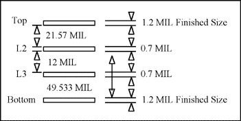
Below is an example of the trace-width calculation for a T3 / E3 LIU interface.
Note: The impedance was calculated with Cadence® Allegro. Basic Network Interface  Layout Considerations Impedance Location—keep termination resistors as close to the LIU as possible. Trace widths—keep trace widths as short as possible. Do not route the GND plane under the transformer to reduce noise. Do not route the VCC plane under the transformer or TXP, TXN, RXP, RXN routes. Isolate the GND plane between board and cable. Layout Examples Example 1: DS3151—The layout of a single-port T3 / E3 LIUTable 1-1. Layout Components
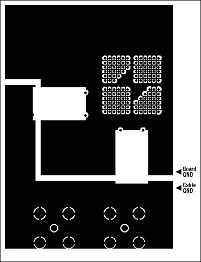
Figure 1-5. DS3151 Single-port, T3 / E3 LIU ground plane {layer two} layout—no ground plane under the transformers.
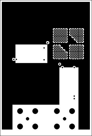
Figure 1-6. DS3151 Single-port, T3 / E3 LIU VCC plane {layer three} layout—no VCC plane under the transformer or TXP, TXN, RXP, RXN.
Example 2: DS3152—The Layout of a Dual-Port T3 / E3 LIUTable 2-1. Layout Components
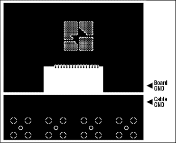
Figure 2-5. DS3152 dual-port, T3 / E3 LIU ground plane {layer two} layout—no ground plane under the transformer.
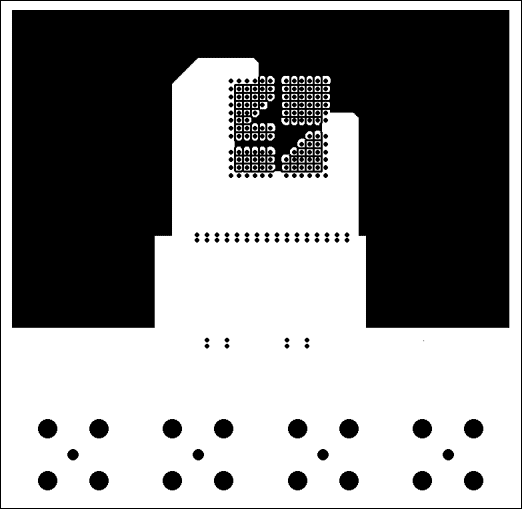
Figure 2-6. DS3152 dual-port, T3 / E3 LIU VCC plane {layer three} layout—no VCC plane under the transformer or TXP, TXN, RXP, RXN.
Example 3: DS3153—The Layout of a Triple-Port, T3 / E3 LIUTable 3-1. Layout Components
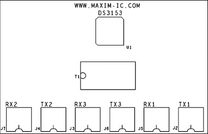
Figure 3-1. DS3153 triple-port, T3 / E3 LIU layout—silkscreen top layer.
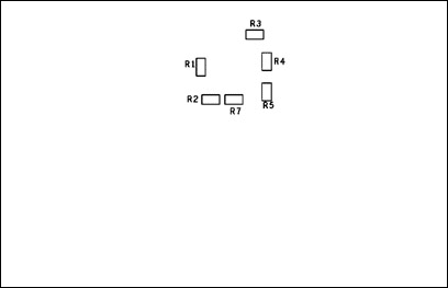
Figure 3-2. DS3153 triple-port, T3 / E3 LIU layout—silkscreen bottom layer (view mirrored).
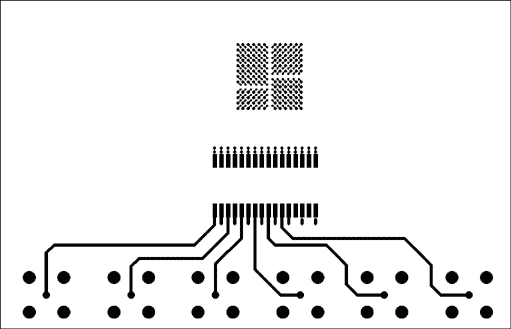
Figure 3-3. DS3153 triple-port, T3 / E3 LIU layout—top conducting layer.
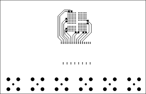
Figure 3-4. DS3153 triple-port, T3 / E3 LIU layout—bottom conducting layer.
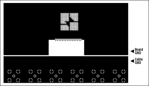
Figure 3-5. DS3153 triple-port, T3 / E3 LIU ground plane {layer two} layout—no ground plane under the transformer.
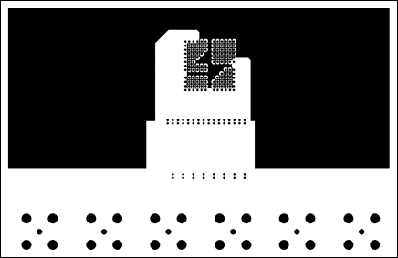
Figure 3-6. DS3153 triple-port, T3 / E3 LIU VCC plane {layer three} layout—no VCC plane under the transformer or TXP, TXN, RXP, RXN.
Example 4: DS3154—The Layout of a Quad-Port, T3 / E3 LIUTable 4-1. Layout Components
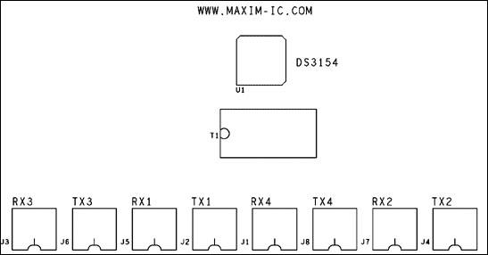
Figure 4-1. DS3154 quad-port, T3 / E3 LIU layout—silkscreen top layer.
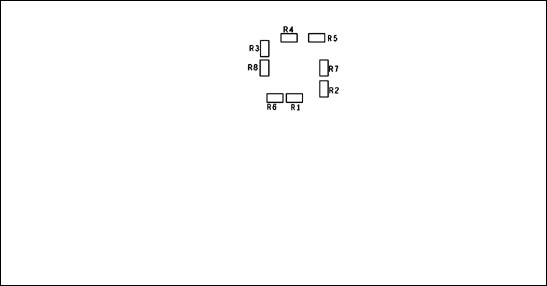
Figure 4-2. DS3154 quad-port, T3 / E3 LIU silkscreen layout—bottom layer (view mirrored).
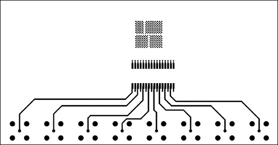
Figure 4-3. DS3154 quad-port, T3 / E3 LIU layout—top conducting layer.
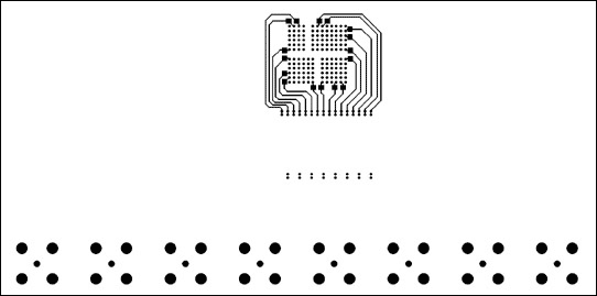
Figure 4-4. DS3154 quad-port, T3 / E3 LIU layout—bottom conducting layer.
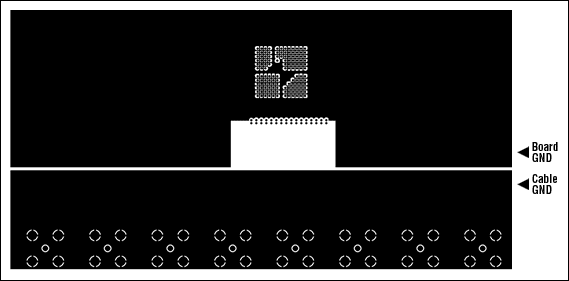
Figure 4-5. DS3154 quad-port, T3 / E3 LIU ground plane {layer two} layout—no ground plane under the transformer.
Figure 4-6. DS3154 quad-port, T3 / E3 LIU VCC plane {layer three} layout—no VCC plane under the transformer or TXP, TXN, RXP, RXN. ConclusionThis application note illustrated what is necessary to maintain the proper impedance for a T3 / E3 networking interface using the DS315x.
If you have further questions about our T3 / E3 products, please contact the Telecommunication Applications support team by email, var name = "telecom.support @"; var domain = "dalsemi"; document.write ("" + name + domain + ""); telecom.support@dalsemi
OverviewThis applicaTIon note is a guideline on how to layout the network interface for Dallas Semiconductor T3 / E3 line interface units (LIUs). The guideline uses the DS315x products as examples. This applicaTIon note is also applicable for other Dallas Semiconductor T3 / E3 products.
The DS315x products include the DS3151 (single), DS3152 (dual), DS3153 (triple), and DS3154 (quad) LIUs which perform the necessary funcTIons for interfacing at the physical layer to a DS3, E3, or STS-1 line. Each LIU has independent receive and transmit paths.
Each layout shows the communication line routing between the DS315x LIU, the transformer, and the 75Ω BNC connectors. In particular, each layout defines the recommended trace widths to ensure the proper impedance for a given network interface. All board stack-ups are the same .
Board Stackup
Below is an example of the trace-width calculation for a T3 / E3 LIU interface.
| Surface Materials | Thickness | Dielectric Constant | Line Widths | Impedance | |
| TX, RX @ 75Ω | |||||
| Top conductor copper | 1.2MIL | N / A | 25MIL | 75Ω | |
| Dielectric FR-4 | 21.57MIL | 4.5 | N / A | N / A | |
| L2_GND conductor copper | 0.7MIL | N / A | N / A | N / A | |
| TXP, TXN, RXP, RXN @ 150Ω | |||||
| Bottom conductor copper | 1.2MIL | N / A | 5MIL | 150Ω | |
| Dielectric FR-4 | 61.53MIL | 4.5 | N / A | N / A | |
| L2_GND conductor copper | 0.7MIL | N / A | N / A | N / A | |
Layout Considerations Impedance Location—keep termination resistors as close to the LIU as possible. Trace widths—keep trace widths as short as possible. Do not route the GND plane under the transformer to reduce noise. Do not route the VCC plane under the transformer or TXP, TXN, RXP, RXN routes. Isolate the GND plane between board and cable. Layout Examples Example 1: DS3151—The layout of a single-port T3 / E3 LIUTable 1-1. Layout Components | Name | Qty | Description | Supplier | Part Number |
| U1 | 1 | Single DS3 / E3 / STS1 LIU, 144P BGA | Dallas Semiconductor | DS3151 |
| C1, C2 | 2 | 0805 Ceram 56000pF, 25V 10% | Panasonic | ECJ-2VB1E563K |
| R1, R2 | 2 | Resistor, 0603 332Ω, 1 / 16W 1% | Panasonic | ERJ-3EKF3320V |
| T1, T2 | 2 | Transformer, 1: 2 T3 / E3 / STS-1, industrial | Pulse | T3012 |
| J1, J2 | 2 | Connector, BNC 75Ω, RA 5-pin | Trompetor | UCBJR220 |
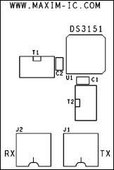 Figure 1-1. DS3151 Single-port, T3 / E3 LIU layout—silkscreen top layer. | 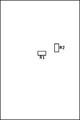 Figure 1-2. DS3151 Single-port, T3 / E3 LIU layout—silkscreen bottom layer (view mirrored). |
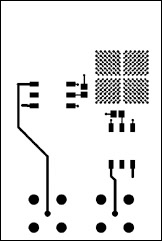 Figure 1-3. DS3151 Single-port, T3 / E3 LIU layout—top conducting layer. | 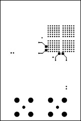 Figure 1-4. DS3151 Single-port, T3 / E3 LIU layout—bottom conducting layer. |
Figure 1-5. DS3151 Single-port, T3 / E3 LIU ground plane {layer two} layout—no ground plane under the transformers.
Figure 1-6. DS3151 Single-port, T3 / E3 LIU VCC plane {layer three} layout—no VCC plane under the transformer or TXP, TXN, RXP, RXN.
Example 2: DS3152—The Layout of a Dual-Port T3 / E3 LIUTable 2-1. Layout Components
| Name | Qty | Description | Supplier | Part Number |
| U1 | 1 | Dual DS3 / E3 / STS1 LIU, 144P BGA | Dallas Semiconductor | DS3152 |
| R1-R4 | 4 | Resistor, 0603 332Ω, 1 / 16W 1% | Panasonic | ERJ-3EKF3320V |
| T1 | 1 | Transformer, OCTAL T3 / E3, 1: 2, SMT 32-pin | Pulse | T3049 |
| J2, J4, J5, J7 | 4 | Connector, BNC 75Ω, RA 5-pin | Trompetor | UCBJR220 |
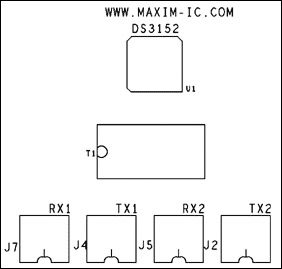 Figure 2-1. DS3152 dual-port, T3 / E3 LIU layout— silkscreen top layer. | 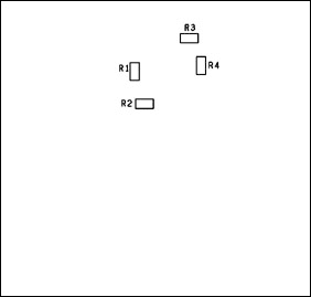 Figure 2-2. DS3152 dual-port, T3 / E3 LIU layout— silkscreen bottom layer (view mirrored). |
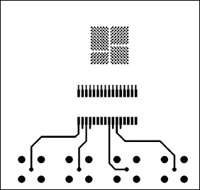 Figure 2-3. DS3152 Dual-port, T3 / E3 LIU layout—top conducting layer. | 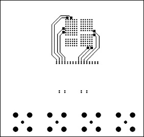 Figure 2-4. DS3152 dual-port, T3 / E3 LIU layout—bottom conducting layer. |
Figure 2-5. DS3152 dual-port, T3 / E3 LIU ground plane {layer two} layout—no ground plane under the transformer.
Figure 2-6. DS3152 dual-port, T3 / E3 LIU VCC plane {layer three} layout—no VCC plane under the transformer or TXP, TXN, RXP, RXN.
Example 3: DS3153—The Layout of a Triple-Port, T3 / E3 LIUTable 3-1. Layout Components
| Name | Qty | Description | Supplier | Part Number |
| U1 | 1 | Triple DS3 / E3 / STS1 LIU, 144P BGA | Dallas Semiconductor | DS3153 |
| R1-R5, R7 | 6 | Resistor, 0603 332Ω, 1 / 16W 1% | Panasonic | ERJ-3EKF3320V |
| T1 | 1 | Transformer, OCTAL T3 / E3, 1: 2, SMT 32-pin | Pulse | T3049 |
| J2-J7 | 6 | Connector, BNC 75Ω, RA 5-pin | Trompetor | UCBJR220 |
Figure 3-1. DS3153 triple-port, T3 / E3 LIU layout—silkscreen top layer.
Figure 3-2. DS3153 triple-port, T3 / E3 LIU layout—silkscreen bottom layer (view mirrored).
Figure 3-3. DS3153 triple-port, T3 / E3 LIU layout—top conducting layer.
Figure 3-4. DS3153 triple-port, T3 / E3 LIU layout—bottom conducting layer.
Figure 3-5. DS3153 triple-port, T3 / E3 LIU ground plane {layer two} layout—no ground plane under the transformer.
Figure 3-6. DS3153 triple-port, T3 / E3 LIU VCC plane {layer three} layout—no VCC plane under the transformer or TXP, TXN, RXP, RXN.
Example 4: DS3154—The Layout of a Quad-Port, T3 / E3 LIUTable 4-1. Layout Components
| Name | Qty | Description | Supplier | Part Number |
| U1 | 1 | Quad DS3 / E3 / STS1 LIU, 144P BGA | Dallas Semiconductor | DS3154 |
| R1-R8 | 8 | Resistor, 0603 332Ω, 1 / 16W 1% | Panasonic | ERJ-3EKF3320V |
| T1 | 1 | Transformer, OCTAL T3 / E3, 1: 2, SMT 32-pin | Pulse | T3049 |
| J1-J8 | 8 | Connector, BNC 75Ω, RA -pin | Trompetor | UCBJR220 |
Figure 4-1. DS3154 quad-port, T3 / E3 LIU layout—silkscreen top layer.
Figure 4-2. DS3154 quad-port, T3 / E3 LIU silkscreen layout—bottom layer (view mirrored).
Figure 4-3. DS3154 quad-port, T3 / E3 LIU layout—top conducting layer.
Figure 4-4. DS3154 quad-port, T3 / E3 LIU layout—bottom conducting layer.
Figure 4-5. DS3154 quad-port, T3 / E3 LIU ground plane {layer two} layout—no ground plane under the transformer.
Figure 4-6. DS3154 quad-port, T3 / E3 LIU VCC plane {layer three} layout—no VCC plane under the transformer or TXP, TXN, RXP, RXN. ConclusionThis application note illustrated what is necessary to maintain the proper impedance for a T3 / E3 networking interface using the DS315x.
If you have further questions about our T3 / E3 products, please contact the Telecommunication Applications support team by email, var name = "telecom.support @"; var domain = "dalsemi"; document.write ("" + name + domain + ""); telecom.support@dalsemi
Cadence is a registered trademark of Cadence Design Systems, Inc.
Battery Formation Charger,Discharger Testing Machine,Battery Formation Machine,Formation Charger/Discharger
Zhijiang BSL battery technology service company , https://www.bslbatteryservice.com