
Abstract: ApplicaTIon note 376 provides the hardware and software requirements for using the DS21Q50 as a quad E1 transceiver. Two significant features are included for this type of applicaTIon, Interleave Bus OperaTIon (IBO) and a system clock synthesizer. IBO mode allows up to eight E1 data streams to be mulTIplexed into a single high-speed PCM bus. The system clock synthesizer can create a high-speed backplane clock based on the recovered clock form any of the E1 lines or an external reference clock.
OverviewThe DS21Q50 is a quad E1 transceiver optimized for high-density termination of E1 lines. Two significant features are included for this type of application: the Interleave Bus Option (IBO) and a system clock synthesizer. The IBO allows up to eight E1 data streams to be multiplexed onto a single high-speed PCM bus. The system clock synthesizer can create a high-speed backplane clock based on the recovered clock from any of the E1 lines, or an externally applied reference clock. Each of these features is accomplished without additional logic components. This document details one specific hardware and software implementation to take advantage of these features for a 4-port E1 design.
Hardware Configuration Figure 1 shows an example application of the DS21Q50 in a 4-port design. In order to ensure data integrity in IBO mode, all clock and sync signals should be phase-aligned. The receive elastic store for each of the four transceivers must be enabled, and they should all receive the same frame-reference pulse (RSYNC) and 8.192MHz system clock (SYSCLK). In this case, the phase-locked frame pulse is provided by the system backplane, and the 8.192MHz clock is provided by the 21Q50's system-clock synthesizer. Note that the 8.192MHz clock can be created internally from any of the four E1 line recovered clocks. In IBO mode, the DS21Q50 can create the transmit clock (TCLK) for each E1 formatter by dividing down the applied SYSCLK.
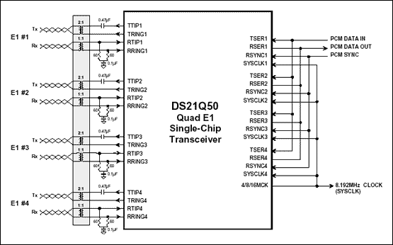
Figure 1. Four port E1 transceiver using DS21Q50.
Notes: Schematic does not include line protection components. For compact applications, an octal transformer can be used such as the Pulse T1068. This circuit can be software-configured for either 75½ or 120½ E1 applications without changing component values: IRTSEL in CCR5.4 determines receiver termination resistance L0-L2 in LICR determines transmitter pulse shape Software Configuration Table 1 shows some of the critical register settings necessary to initialize the DS21Q50 for operation as described above. Note that Table 1 might not represent the complete register listing required for a customer application . The reader is encouraged to refer to the device data sheet for further information regarding the flexibility of the DS21Q50. It is good practice to clear all 21Q50 registers at power-up, before initializing the device with the desired settings.
Table 1. Register Settings for 21Q50 4-Port Design
Where:
TC # 1 = Transceiver # 1 (TS1, TS0 = 00)
TC # 2 = Transceiver # 2 (TS1, TS0 = 01)
TC # 3 = Transceiver # 3 (TS1, TS0 = 10)
TC # 4 = Transceiver # 4 (TS1, TS0 = 11)
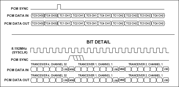
Figure 2. PCM Bus functional timing diagram.
OverviewThe DS21Q50 is a quad E1 transceiver optimized for high-density termination of E1 lines. Two significant features are included for this type of application: the Interleave Bus Option (IBO) and a system clock synthesizer. The IBO allows up to eight E1 data streams to be multiplexed onto a single high-speed PCM bus. The system clock synthesizer can create a high-speed backplane clock based on the recovered clock from any of the E1 lines, or an externally applied reference clock. Each of these features is accomplished without additional logic components. This document details one specific hardware and software implementation to take advantage of these features for a 4-port E1 design.
Hardware Configuration Figure 1 shows an example application of the DS21Q50 in a 4-port design. In order to ensure data integrity in IBO mode, all clock and sync signals should be phase-aligned. The receive elastic store for each of the four transceivers must be enabled, and they should all receive the same frame-reference pulse (RSYNC) and 8.192MHz system clock (SYSCLK). In this case, the phase-locked frame pulse is provided by the system backplane, and the 8.192MHz clock is provided by the 21Q50's system-clock synthesizer. Note that the 8.192MHz clock can be created internally from any of the four E1 line recovered clocks. In IBO mode, the DS21Q50 can create the transmit clock (TCLK) for each E1 formatter by dividing down the applied SYSCLK.
Figure 1. Four port E1 transceiver using DS21Q50.
Notes: Schematic does not include line protection components. For compact applications, an octal transformer can be used such as the Pulse T1068. This circuit can be software-configured for either 75½ or 120½ E1 applications without changing component values: IRTSEL in CCR5.4 determines receiver termination resistance L0-L2 in LICR determines transmitter pulse shape Software Configuration Table 1 shows some of the critical register settings necessary to initialize the DS21Q50 for operation as described above. Note that Table 1 might not represent the complete register listing required for a customer application . The reader is encouraged to refer to the device data sheet for further information regarding the flexibility of the DS21Q50. It is good practice to clear all 21Q50 registers at power-up, before initializing the device with the desired settings.
Table 1. Register Settings for 21Q50 4-Port Design
| Setting | Location | Description |
| The following settings apply to all 4 ports (transceivers): | ||
| IBOEN = 1 | IBO.2 | Enable IBO operation |
| IBOTCS = 1 | IBO.6 | Transmit clock derived from SYSCLK |
| SCS1 = 1 | IBO.5 | 8.192MHz operation (4 ports on the PCM bus) |
| SCS0 = 0 | IBO.4 | |
| RESE = 1 | RCR.4 | Enable receive elastic store |
| RSIO = 1 | RCR.5 | RSYNC pin is an input |
| RSM = 0 | RCR.6 | RSYNC is in frame mode |
| TSIO = 1 | TCR.0 | TSYNC is an output |
| TSM = 0 | TCR.1 | TSYNC is in frame mode |
| The following settings apply to the specified port (transceiver): | ||
| SCS0 = 1 | TC # 1, SCICR.0 | Select the recovered clock from transceiver # 1 as the source for the system clock synthesizer |
| SCS1 = 0 | TC # 1, SCICR.1 | |
| SCS2 = 0 | TC # 1, SCICR.2 | |
| CSS0 = 0 | TC # 1, SCICR.3 | Set system clock synthesizer to 8.192MHz |
| CSS1 = 1 | TC # 1, SCICR.4 | |
| SOE = 1 | TC # 1, SCICR.5 | Enable synthesizer clock output |
| DA0 = 0 | TC # 1, IBO.0 | Set transceiver # 1 as first device on PCM bus |
| DA1 = 0 | TC # 1, IBO.1 | |
| DA2 = 0 | TC # 1, IBO.2 | |
| DA0 = 1 | TC # 2, IBO.0 | Set transceiver # 2 as second device on PCM bus |
| DA1 = 0 | TC # 2, IBO.1 | |
| DA2 = 0 | TC # 2, IBO.2 | |
| DA0 = 0 | TC # 3, IBO.0 | Set transceiver # 3 as third device on PCM bus |
| DA1 = 1 | TC # 3, IBO.1 | |
| DA2 = 0 | TC # 3, IBO.2 | |
| DA0 = 1 | TC # 4, IBO.0 | Set transceiver # 4 as fourth device on PCM bus |
| DA1 = 1 | TC # 4, IBO.1 | |
| DA2 = 0 | TC # 4, IBO.2 | |
Where:
TC # 1 = Transceiver # 1 (TS1, TS0 = 00)
TC # 2 = Transceiver # 2 (TS1, TS0 = 01)
TC # 3 = Transceiver # 3 (TS1, TS0 = 10)
TC # 4 = Transceiver # 4 (TS1, TS0 = 11)
Figure 2. PCM Bus functional timing diagram.
Super Silent Cummins Diesel Generator
Cummins Genset,Super Silent Cummins Diesel Generator,Diesel Generator With Cummins Engine,Cummins Silent Diesel Generator
Jiangsu Lingyu Generator CO.,LTD , https://www.lygenset.com