
Due to the continuous development of single-chip technology and the emergence of high-brightness LED lighting tubes, large-screen high-brightness LED electronic advertising screens have become possible. Compared with traditional neon advertising, LED electronic advertising screen has incomparable advantages in display effect and modifiability, and the increasingly popularization of single-chip microcomputer and the continuous innovation of LED technology make high-brightness and high-definition LED dot matrix advertisement Cards are increasingly close to the cost of traditional neon billboards. In addition, the rapid development of SMT technology, the large-scale use of switching power supply, it has obvious advantages in terms of volume and reliability than traditional neon advertising, laying the foundation for its application in special fields.
1 Design principle and design plan
1.1 Design principle
For the dot matrix LED display, a common cathode or a common anode can be used. The system uses a common anode, and its hardware circuit is shown in FIG. When there is a positive strobe signal on the line, the LED with the four bits of data at the column selection is turned on. In this way, it is only necessary to scan the display code of the graphic or text as a column signal and the corresponding line signal, so that the dot matrix can be illuminated line by line. As long as the scanning speed is greater than 24 Hz, the scanning time is very fast, and the human eye's vision has a temporary effect, and it can be seen that the full graphic or text is displayed.
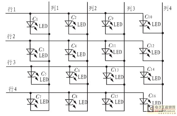
Figure 1 hardware circuit
This design is to complete the design of LED dot matrix display control based on single chip microcomputer. The overall scheme is to use single chip as the control core, and display the text on the LED dot matrix screen by means of static, left shift and right shift through the row and column drive circuit. In the design process, the driving circuit uses dynamic scanning display. The dynamic scanning is simply to turn on the line by line, so that the scanning drive circuit can realize a row driver of the same name column of multiple lines (such as 16 lines). Due to the limitation of dynamic scanning display (parallel transmission), dynamic scanning display (serial transmission) is adopted, and the display mode uses the LED dot matrix screen module as a display screen.
1.2 Overall plan
The design of the single-chip microcomputer adopts AT89C51, the line circuit uses the progressive scan mode, the column circuit uses the serial data transmission mode, and the display screen uses a dot matrix module composed of 16x16 dot matrix LEDs. The chip used has an incoming and outgoing shift register 74LS595, a 4-wire-16 line decoder 74LS154 and a triode 8550. The overall design block diagram is shown in Figure 2.
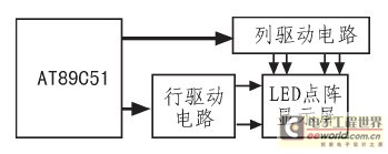
Figure 2 Overall design block diagram
2 system hardware design
The hardware circuit can be roughly divided into a single-chip system and peripheral circuits, column drive circuits and row drive circuits, and LED dot matrix arrays. The chips used are single-chip AT89C51, 4-wire-16-line decoder 74LS154, with latch function. String in and out of shift register 74LS595.
2.1 SCM system and peripheral circuits
The one-chip computer adopts AT89C51. The system uses a crystal of 12 MHz or higher to achieve a higher refresh rate for a more stable display. The single-chip serial port is connected to the column driver for sending display data. The lower 4 bits of the P1 port are connected to the row driver, and the row selection signal is sent, and the P1.5 to P1.7 ports are used to transmit the control signal. The P0 and P2 ports are free, and the ROM and RAM of the system can be expanded as necessary.
2.2 Clock pulse circuit
AT89C51's highest clock frequency has reached 24 MHz, it has an internal oscillation circuit, as long as the two pins of the AT89C51 (ie, 19, 18 feet) are connected to the two pins of a simple quartz crystal, while The two pins of the crystal are also coupled to ground with a 30 pF capacitor, as shown in Figure 3.
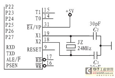
Figure 3 clock pulse circuit
2.3 reset circuit
The reset pin (RESET) of the AT89C51 is the 9th pin. When this pin is connected high for more than 2 machine cycles, the reset action can be generated. Taking a 24 MHz clock pulse as an example, each clock pulse is 05 μs, and the two machine cycles are 1 μs. Therefore, a 2 μs high-level pulse is connected to the 9th pin to generate a reset action. The simplest is that only one resistor and one capacitor can form a reliable reset circuit. The resistor is generally 10 kΩ, and the capacitor is generally 10 μF, as shown in Figure 4.
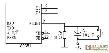
Figure 4 reset circuit
2.4 dot matrix display driver circuit design
Because the problem requires that the integrated drive circuit is not allowed, but the drive circuit is not used, the display is unstable and the brightness is not high. Therefore, the discrete component transistor is used as the drive circuit, and the drive circuit is as shown in FIG. 5.
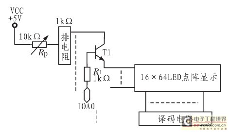
Figure 5 dot matrix display drive circuit
3 system software design
The main function of the display software is to provide display data to the display and generate various control signals to display the screen according to the design requirements.
According to the principle of hierarchical design of software, the software system of the display screen can be divided into two layers: the first layer is the underlying display driver, and the second layer is the upper layer system application. The display driver is responsible for transmitting the specific combined display data to the dot matrix screen, and is responsible for generating the line scan signal and other control signals to complete the scan display operation of the LED display screen. The display driver is implemented by the display subroutine; the system environment setting (initialization) is completed by the system initialization program; the display effect processing and the like are performed by the main program by calling the subroutine.
3.1 display driver
After the display driver enters the interrupt, it must first re-assign the initial value of the timer T0 to ensure the stability of the display refresh rate. The display refresh rate (frame rate) of the 16-line scan format is calculated as follows:

Where: F is the crystal frequency; T is the initial value of the timer T0 (operating in the 16-bit timer mode).
Secondly, the display driver queries the currently lit line number, reads the display data of the next line from the display buffer area, and sends it to the shift register through the serial port.
In order to eliminate the smearing caused when the data is displayed in the switching line, the driver first needs to turn off the display, that is, blanking, and after displaying the data input/output latch, output a new line number and re-open the display. Figure 6 shows the flow chart of the display driver (display scan function).
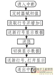
Figure 6 shows the driver flow chart
3.2 System main program
After the system main program starts, it first initializes the system environment, including setting the serial port, timer, interrupt, and port. Then display the text or pattern with the "rolling out" effect, stay for a few seconds, then scroll up to display the Chinese characters or graphics, stay for a few seconds, then move left to display Chinese characters or graphics, right shift display, and so on. Finally, the text is hidden by the "rolling curtain" effect. Figure 7 shows the flow chart of the main program of the system.
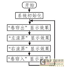
Figure 7 Flow chart of the main program of the system
4 software simulation and hardware implementation
4.1 Software Simulation
The core unit of this design is the single-chip AT89C51, so the single-chip simulation software Proteus 7.O and Keil are used to simulate the whole design.
Run the ISIS module in Proteus to layout the designed schematic. The simulation circuit is shown in Figure 8.
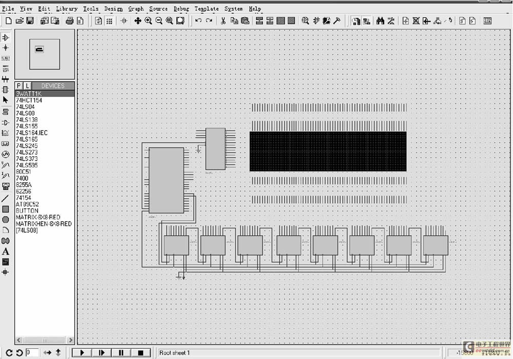
Figure 8 simulation circuit
Copy the complete source program to the Keil simulation development environment and run the debugger. Load the compiled source program into the simulation circuit diagram, run the program, and press the "drawing curtain", "left roller blind", "right roller blind", "rolling curtain" on the dot matrix display according to the design display effect. "The results are correct.
4.2 Hardware Implementation
After the software simulation is passed, the correctness and feasibility of the scheme are fully proved. According to the design scheme, the hardware circuit is built and debugged. The result is as shown in Figure 9 below.
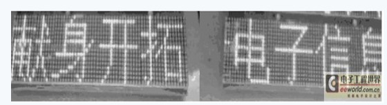
Figure 9 hardware physical map
5 Conclusion
In this paper, by designing the design of LED dot matrix display control based on single chip microcomputer, the LED display module unit is studied in the process of row signal control and signal transmission. The principle of the hardware and the connection method, the software design flow and part of the code are given, and the complete circuit diagram is given. The result can display Chinese characters and picture information normally, and can display dynamically.
Edit: Nizi
China leading manufacturers and suppliers of Smart Solar Street Light,Solar Street Lighting System, and we are specialize in Integrated Solar Street Light,All In One Solar Street Light, etc.
Solar Street Light
Smart Solar Street Light,Solar Street Lighting System,Integrated Solar Street Light,All In One Solar Street Light
Jiangmen Liangtu Photoelectric Technology Co., Ltd. , https://www.liangtulight.com