
Abstract: This paper presents a stereo audio interface design based on the Kinetis MK60N512 microcontroller and the 16-bit/24-bit audio digital-to-analog converter MAX5556. The MK60N512 transmits audio data from the I2S bus to the MAX55 56. The output audio signal is filtered by an active filter to ensure the audio quality while improving its load capacity. The MK60N512's internal high-performance programmable enhanced DMA transfers audio data to the I2S module, reducing the burden on the microcontroller core.
Key words: Kinetis; MK60N512; MAX5556; enhanced DMA; I2S bus
Introduction The MK60N512 is the most integrated chip of Freescale's Kinetis family of microcontrollers. It is based on the ARM Cortex-M4 core and features low power consumption, high performance and low cost for embedded audio, automotive electronics and power supplies. Management provides flexible solutions. The MAX5556 is a low-power, stereo audio digital-to-analog converter (DAC) from Maxim that supports the standard I2S bus protocol with sampling accuracy of up to 24 bits and a sample rate of 2 to 50 kHz. The ∑-Δ modulation technique can effectively shape the quantization noise and reduce the quantization noise.
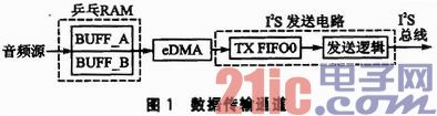
In the audio processing system, DMA is used to realize the transmission of audio data in the microcontroller, which can reduce the participation of the kernel and reduce the burden on the core. The data transmission channel of the system is shown in Figure 1. The audio signal is temporarily stored in the buffer area and transmitted by the DMA to the transmission circuit of the I2S bus module. In order to maintain the continuity of the audio signal, the "ping-pong RAM" is used to design the cache. In the figure, A/B indicates the number of the ping-pong RAM.
This article refers to the address: http://
1 MK60N512 I2S bus and eDMA introduction
1.1 I2S bus module MK60N512 I2S bus module has three basic operating modes: normal mode, network mode and gated clock mode. For audio applications, the I2S bus module also supports two derivative modes: I2S bus mode and AC97. mode. The structure of the I2S bus module is as shown in FIG. 2, and is composed of a transmitting circuit, a receiving circuit, a serial clock, and a frame synchronous clock generating circuit. STCK and SRCK are serial transmission and reception clock ports, STFS and SRFS are serial transmission and reception frame synchronization ports, and STXD and SRXD are serial transmission and reception data ports. In the synchronous mode, the STCK port is used by the transmitting and receiving units.
Both the transmit and receive circuits have two FIFOs with a width of 32 bits and a depth of 15. These FIFOs can be accessed by writing to and reading the transmit data registers TX0/TX1 and receive data registers RX0/RX1. The transmit logic transfers the data in the TX FIFO, loads the transmit serial shifter TXSR, and then serially transmits it from the STXD port; the receive logic shifts the data out of the incoming data frame and places them in the receive RXFIFO. Entrance. When the TX FIFO is missing or the RX FIFO data reaches the set number, an interrupt or DMA transfer is triggered.
1.2 eDMA
The MK60N512's eDMA is highly programmable, and data transfer is highly optimized with virtually no CPU core intervention. Unlike normal DMA, eDMA transfers consist of a main loop and a minor loop (MinorLoop). The main loop is automatically triggered by the peripheral. After each main loop, the source address and destination address are automatically offset according to the values ​​in the TCDn_SOFF and TCDn_DOFF registers without the need for the CPU to modify. In addition to all interrupt requests after the end of the transfer, eDMA also supports "half-interrupt", that is, the main loop completes the interrupt request when half of the total number of cycles is completed, which is especially suitable for the "ping-pong RAM" design.
2 Introduction to MAX5556
2.1 Pin Definition and Internal Structure The internal structure of MAX5556 is shown in Figure 3. MCLK is the main clock, LRCLK is the left/right channel selection clock, SCLK is the external serial clock, SDATA is the serial audio input, OUTL/OUTR Output for left/right channel. After the serial interface module acquires the audio data, it is filtered by the built-in digital interpolator and filter to remove the harmonic noise carried by the baseband audio signal; the audio data is modulated by the DAC after being modulated by the ∑-Δ modulator, and the output is simulated. The signal is filtered by an internal analog low-pass filter that attenuates high-frequency quantization noise; the built-in output buffer can drive load resistors greater than 3 kΩ and load capacitances up to 100 pF; the final analog audio signal is output from OUTL/OUTR.
2.2 Operating Modes The MAX5556 supports external serial clock mode and internal serial clock mode. In a LRCLK cycle, if a valid SCLK is detected, the external serial clock mode is entered, SCLK is used as the sampling clock; if no valid SCLK is detected, the internal serial clock mode is entered and the sampling clock is internally generated. The frequency of the internal sampling clock is determined by the ratio of the detected MCLK to LRCLK. If the ratio of MCLK to LRCLK is 384, the internal sampling clock frequency is 48 × fLRCLK; if the ratio of MCLK to LRCLK is 256 or 512, the internal sampling clock The frequency is 32 × fLRCLK.
2.3 Data Format The MAX5556 supports left-justified 16-bit or 24-bit data formats. When it is operating in the external serial clock mode, or operating in the internal serial clock mode, and the ratio of MCLK to LRCLK is 384, the valid data is 24 bits. If the data is less than 24 bits, the low bits fill zero; more than 24 bits of data are ignored. When operating in the internal serial clock mode and the ratio of MCLK to LRCLK is 256 or 512, the valid data is 16 bits. The data format of the MAX5556 is shown in Figure 4. Each time the LRCLK edge changes the second SCLK rising edge, the data on SDATA begins to be valid, the most significant bit (MSB) appears; the least significant bit (LSB) appears after 24 or 16 clock cycles. When LRCLK is 0, the data enters the left channel DAC; when LRCLK is 1, the data enters the right channel DAC.
3 system hardware circuit design MK60N512 through the I2S bus to transmit audio data to the MAX5556 for digital-to-analog conversion, the output analog audio signal is filtered by the filter circuit, while improving the load capacity. The I2S bus module works in the I2S bus master mode. The pins corresponding to the STCK, STFS, and STXD ports of the transmit circuit are BCLK, TX_FS, and TXD, respectively. The main clock of the I2S bus module is output through the MCLK pin. The hardware circuit is shown in Figure 5. Since the MK60N512 operates at 3.3 V and the MAX5556 operates at 5 V, the interface is pulled up to improve data transmission stability.
The LM358 has an effective output of 1.5 to 3.5 V when operating from a single 5 V supply, while the output of the MAX5556 can reach 0 to 5 V. Therefore, the original signal is attenuated at the input using R1 and R2 to prevent the output signal from being cut. Top distortion.
4 software design
4.1 "Ping Pong RAM" Design The I2S bus module of the MK60N512 supports two channels in the I2S bus mode. The audio data is interleaved in the FIFO, so the audio data in the buffer also needs to be interleaved. The data cache is shown in Figure 6, where L/R represents the audio left/right channel. Each audio data occupies 4 bytes of space. The buffers BUFF_A and BUFF_B are continuous at the physical address. They are all 512 bytes in size and store a total of 256 audio data. When the DMA reads data from the buffer BUFF_A, the CPU stores the next set of audio signals in the buffer BUFF_B; when the DMA transfers all the data in the BUFF_A, the DMA channel source address is switched to BUFF_B, and the CPU goes to BUFF_A. Store data, so iterative.
4.2 I2S bus module configuration configuration I2S bus module works in the I2S bus master mode, the default one frame data length is 32 bits, and is left-aligned mode; use frame synchronization TX_FS as the channel selection clock, and the synchronization frame length is One word. Since the SCLK signal of the MAX5556 is provided by the MK60N512, the MAX5556 operates in an external serial clock mode with a valid data bit of 24 bits, thus configuring the transmit data bit to be 24 bits. According to the data format of the MAX5556, data needs to be output from the TXD data on the falling edge of SCLK, and the early frame synchronization needs to be sent, the data is delayed by one sampling clock, and the frame frequency needs to be set according to the audio sampling frequency.
Enable TX FIFO and its DMA request, start DMA main loop when FIFO hollow number reaches 8. Figure 7 shows the audio data moving process in the TXFIFO. In Figure 7(a), the FIFO is full. As the transmit shift logic fetches a data from the FIFO, the FIFO generates a gap, as shown in Figure 7(b). When 8 times of data is sent, the number of FIFO vacancies reaches 8, triggering the DMA main transmission, as shown in Figure 7(c).
The initialization code of the I2S bus is slightly - editor's note.
4.3 eDMA configuration When the TX FIFO vacancy number reaches 8, trigger DMA main loop, so the number of data transferred per main loop is 32 bytes, the source address offset of each main loop is also 32 bytes, complete buffer area 1 024 Byte data transfer requires 32 main loops. At the end of the 16th main loop, the DMA has transferred all the data in BUFF_A, the DMA source address points to BUFF_B, and generates a "semi-interrupt" request. The CPU starts to store the next set of 512 bytes of audio data to BUFF_A.
When the data transfer in BUFF_B ends, the source address is restored to the BUFF_A start address, and an interrupt request is generated. The CPIJ responds to the interrupt and stores the next set of 512 bytes of audio data to the BIJFFB. It can be seen that during the transfer, the CPU only needs to respond to the interrupt request twice and then write the audio data to the buffer area. The source address is offset by 32 bytes after each main loop. After the complete transfer is completed, the source address is restored to the BUFF_A start address. These operations are performed by the eDMA module itself.
The initialization code of the DMA is slightly - editor's note.
5 Test Results Figure 8 shows the waveforms of TX_FS and TXD. Channel 1 is TX_FS and Channel 2 is TXD. The audio data sent by the left/right channel is 0x555. The transmission frame frequency of Fig. 8(a) is 48 kHz, and Fig. 8(b) is 44.1 kHz. As can be seen from Figure 8, the data length is 24 bits, left-justified mode, and the data and frame synchronization has a sampling clock delay, in line with the MAX5556 data format and timing.
Conclusion This paper designed a stereo audio interface based on Kinetis MK60N512 and MAX5556. The MK60N512 transmits audio data to the MAX5556 via the I2S bus according to the data format and timing of the MAX5556. The MAX5556 internal DAC converts the data into an analog signal output, and the filter circuit pairs the audio signal. Filtering while improving load capacity. Use MK60N512 internal high-performance configurable eDMA to increase system data transfer rate and reduce CPU load. Tests show that the system can output stereo audio with adjustable output frequency, which can provide reference for Kinetis series microcontroller audio solutions.
Vacuum Cleaner is a tool to help people clean clearly. It can help people to save time and energy. So every family can own one style at least. Now I will introduce something about vacuum cleaners in our factory.There are some kinds of vacuum cleaners in our factory. For example, Car Vacuum Cleaner,Handheld Vacuum Cleaner,Cyclone Vacuum Cleaner,Water filter Drum Vacuum Cleaner and so on. They all have their own features. For example,car vacuum cleaner can use in the car,you can take it to anywhere by car. When your car is dirty,you can clean the car by it. Handheld vacuum cleaner is light weight and convenient,it is easy to use. Cyclone vacuum cleaner is beautiful with high suction power. So it can clean more thoroughly. Any others also have their own features. I will explain in the next moment. Now let's see some pictures.


Vacuum Cleaner
Portable Vacuum Cleaner, Rechargeable Vacuum Cleaner, Hand Vacuum Cleaner, Bagless Vacuum Cleaner
Ningbo ChinaClean Household Appliances Manufacture Co., Ltd. , https://www.chinaclean-elec.com