
Oscillator BasicsThe oscillator used in Dallas Semiconductor RTCs is a CMOS inverter variation of a Pierce-type oscillator. Figure 1 shows a general configuration. These RTCs include integrated load capacitors (CL1 and CL2) and bias resistors. The Pierce oscillator utilizes a crystal operating in parallel-resonance mode. Crystals used in parallel-resonance mode will be specified for a certain frequency with a specific load capacitance. For the oscillator to run at the correct frequency, the oscillator circuit must load the crystal with the correct capacitive load.
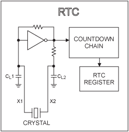
Figure 1. RTC oscillator with internal load capacitors and bias resistors. AccuracyThe frequency accuracy of a crystal-based oscillator circuit is mainly dependent upon the accuracy of the crystal and the accuracy of the match between the crystal and the oscillator capacitive load. If the capacitive load is less than the crystal was designed for, the oscillator runs fast. If the capacitive load is greater than what the crystal was designed for, the oscillator runs slow.
In addition to the errors from the crystal and the load match, crystals vary from their base frequency as the ambient temperature changes. Dallas RTCs use "tuning fork" crystals, which exhibit an error over temperature, as shown in Figure 2. An error of 20ppm is equivalent to approximately 1 minute per month.
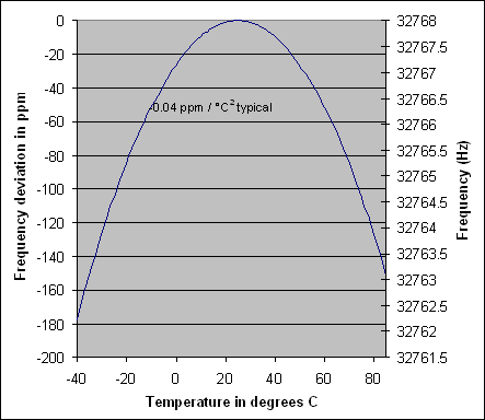
Figure 2. Crystal frequency vs. temperature.
Note: If better accuracy is required, a TCXO such as the DS32kHz can be used.
Crystal Parameters Figure 3 shows the equivalent circuit for a crystal. Near the resonate frequency the circuit consists of a series circuit including motional inductance L1, motional resistance R1, and motional capacitance C1. The parallel component CO is the shunt capacitance of the crystal.
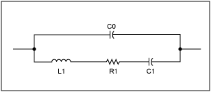
Figure 3. Crystal equivalent circuit.
The load capacitance CL is the capacitive load of the oscillating circuit as seen from the pins of the crystal. Figure 4 shows CL as a capacitance in parallel with the crystal. The load capacitors used in an oscillator circuit, CL1 and CL2, plus any stray capacitance in the circuit, combine to create the overall load capacitance. All Dallas RTCs have integrated CL1 and CL2 capacitors. Care should be taken to minimize stray capacitance in the PC board layout. The following formula shows the relationship between CL and load capacitor values:
CL = [(CL1 × CL2) / (CL1 + CL2) + CSTRAY]
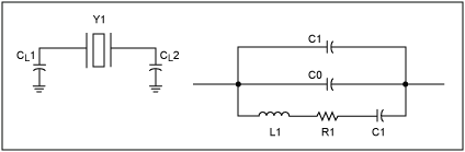
Figure 4. Crystal load capacitors and equivalent parallel load.
Most crystals allow a maximum drive level of 1µW. All Dallas RTCs run under 1µW. Drive level may be determined using the following formula:
P = 2R1 × [π × 32,768 (CO + CL) VRMS] ²,
where VRMS is the RMS value of the voltage across the crystal.
Oscillator Startup Time Oscillator startup times are highly dependent upon crystal characteristics, PC board leakage, and layout. High ESR and excessive capacitive loads are the major contributors to long startup times. A circuit using a crystal with the recommended characteristics and proper layout usually starts within one second.
Table 1. Crystal Specifications
| Parameter | Symbol | Min | Typ | Max | Units |
| Nominal Frequency | FO | 32.768 | kHz | ||
| Frequency Tolerance | delta F / FO | ± 20 | ppm | ||
| Load Capacitance | CL | 6 | pF | ||
| Temperature Turnover Point | T0 | 20 | 25 | 30 | ° C |
| Parabolic Curvature Constant | k | 0.042 | ppm / ° C | ||
| Quality Factor | Q | 40,000 | 70,000 | ||
| Series Resistance | ESR | 45 | kΩ | ||
| Shunt Capacitance | C0 | 1.1 | 1.8 | pF | |
| Capacitance Ratio | C0 / C1 | 430 | 600 | ||
| Drive Level | DL | 1 | µW |
Table 2. Crystal Suppliers, cylinder-type (ESR = 45KΩ)
| Manufacturer | Part | Frequency Tolerance (ppm) | ESR (KΩ) | Drive Level max (µW) | CL-pF | Alternate CL? | Temp Range (° C) | Surface or Thru-Hole | Package Dimensions (mm) | Manufacturer Ordering Number |
| Citizen | CFS-145 | ± 20 | 40 | 1.0 | 8.0 | yes | -10 to +60 | TH | 1.5 x 5.1 | |
| Citizen | CFS-206 | ± 20 | 35 | 1.0 | 12.5 | yes | -10 to +60 | TH | 2.1 x 6.2 | |
| Citizen | CMR-200T | ± 20 | 35 | 1.0 | 12.5 or 6.0 | yes | -40 to +85 | SMT | 2.0 X 6.0 | CMR200TB32.768KDZFTR or CMR200TB32.768KDZBTR |
| ECS, Inc. | ECS-3X8 | ± 20 | 35 | 1.0 | 12.5 | ? | -10 to +60 | TH | 3.1 x 8.2 | |
| ECS, Inc. | ECS-2X6 | ± 20 | 35 | 1.0 | 12.5 | ? | -10 to +60 | TH | 2.1 x 6.2 | |
| ECS, Inc. | ECS-1X5 | ± 20 | 35 | 1.0 | 8 | ? | -10 to +60 | TH | 1.5 x 5.1 | |
| KDS / Daiwa | DT-26 | ± 20 or ± 30 | 40 | 1.0 | 12.5 | yes | -10 to +60 | TH | 2.0 x 6.0 | 1TB602G00 |
| KDS / Daiwa | DT-38 | ± 20 or ± 30 | 30 | 1.0 | 12.5 | yes | -10 to +60 | TH | 3.0 x 8.0 | |
| Pletronics | WX15 | ± 20 | 40 | 1.0 | 8.0 | yes | -10 to +60 | TH | 1.5 x5.1 | WX15-32.768k-6pF |
| Pletronics | WX26 | ± 20 | 40 | 1.0 | 12.5 | 6.0 | -10 to +60 | TH | 2.1 x 6.2 | WX26-32.768k-6pF |
| Fox | NC-38 | 35 | 1.0 | 12.5 | 6.0 | -20 to +60 | TH | 3.0 x 8.3 | ||
| Seiko | C-001R | ± 20 | 45 | 1.0 | 12.5 | 6 | -10 to +60 | TH | 3.1 x 8.0 | |
| Seiko | C-2 | ± 20 | 35 | 1.0 | 12.5 | 6 | -10 to +60 | TH | 2.0 x 6.0 |
Table 3. Crystal Suppliers, Surface Mount
| Manufacturer | Part | Frequency Tolerance (ppm) | ESR (kΩ) | Drive Level max (µW) | CL-pF | Alternate CL? | Temp Range (° C) | Dimensions (mm) approximate, including leads |
| Seiko | SP-T3 | ± 10, ± 20 | 55 | 1.0 | 12.5 | yes | -40 to +85 | 7.3x4.3.x1.8 |
| Seiko | SP-T2 | ± 20 | 50 | 1.0 | 12.5 | yes | -40 to +85 | 8.7x3.7x2.5 |
| EPSON | MC-306 | ± 20 | 50 | 1.0 | 12.5 | yes | -40 to +85 | 8.0x3.8x2.54 |
| Citizen | CM200S | ± 20 | 50 | 1.0 | 12.5 | yes | -40 to +85 | 8.0x3.8x2.5 |
| KDS | DMX-26S | ± 30 | 50 | 1.0 | 12.5 | yes | -40 to +85 | 8.0x3.8x2.4 |
http: //
http: //
http: //XTAL.htm#32
http: //
http: //
Power ConsumptionMany RTCs are designed to operate from a battery supply. In a typical application, a small lithium battery can be used to run the oscillator and clock circuitry while the main supply is off. To maximize battery life, the oscillator must run using as little power as possible. To accomplish this, some design tradeoffs must be made.
Negative ResistanceFor typical high-frequency oscillator circuits, it is normal for the circuit to be designed with a 5 or 10X margin for the ESR. Low-frequency crystals typically have higher ESRs. An RTC oscillator may have less than a 2X margin for negative resistance . An oscillator circuit with a low margin normally consumes less current. As a result, an RTC oscillator often is sensitive to relatively small amounts of stray leakage, noise, or an increase in ESR.
The CL of the oscillator circuit influences the power consumption. An RTC with 12.5pF internal loads consumes more power than one that has 6pF loads. However, the oscillator with 12.5pF load capacitors is usually less susceptible to noise.
Crystal Layout GuidelinesSince the crystal inputs of Dallas RTCs have very high impedance (about 109Ω), the leads to the crystal act like very good antenna, coupling high-frequency signals from the rest of the system. If a signal is coupled onto the crystal pins , it can either cancel out or add pulses. Since most of the signals on a board are at a much higher frequency than the 32.768kHz crystal, it is more likely to add pulses where none are wanted. These noise pulses get counted as extra clock "ticks" and make the clock appear to run fast.
The following steps illustrate how to determine if noise is causing the RTC to run fast: Power the system up and synchronize the RTC to a known accurate clock. Turn the system power off. Wait for a period of time (two hours, 24 hours, etc.). The longer the time period, the easier it is to measure the accuracy of the clock. Turn the system on again, read clock, and compare to the known accurate clock. Resynchronize the RTC to the known accurate clock. Keep the system powered up and wait for a period of time equal to the period in Step 3. Read the clock after waiting for the above period of time and compare it to the known accurate clock. By using the above steps, the accuracy of the clock can be determined both when the system is powered up and when the system is powered down. If the clock proves to be inaccurate when the system is powered up, but is accurate when the system is powered down, the problem is most likely due to noise from other signals in the system. However, if the clock is inaccurate both when the system is powered up and when it is powered down, then the problem is not due to noise from the system.
Since it is possible for noise to be coupled onto the crystal pins, care must be taken when placing the external crystal on a PC board layout. It is very important to follow a few basic layout guidelines concerning the placement of the crystal on the PC board layout to ensure the extra clock ticks do not couple onto the crystal pins. It is important to place the crystal as close as possible to the X1 and X2 pins. Keeping the trace lengths between the crystal and RTC as small as possible reduces the probability of noise coupling by reducing the length of the antenna. Keeping the trace lengths small also decreases the amount of stray capacitance. Keep the crystal bond pads and trace width to the X1 and X2 pins as small as possible. The larger these bond pads and traces are , the more likely it is that noise can couple from adjacent signals. If possible, place a guard ring (connected to ground) around the crystal. This helps isolate the crystal from noise coupled from adjacent signals. See Figure 2 for an illustration of using a guard ring around a crystal. Try to ensure that no signals on other PC board layers run directly below the crystal or below the traces to the X1 and X2 pins. The more the crystal is isolated from other signals on the board, the less likely it is that noise is coupled into the crystal. There should be a minimum of 0.200 inches between any digital signal and any trace connected to X1 or X2. The RTC should be isolated from any component that generates electromagnetic radiation (EMR). This is true for discrete and module type RTCs. It may also be helpful to place a local ground plane on the PC board layer immediately below the crystal. This helps to isolate the crystal from noise coupling from signals on other PC board layers. Note that the ground plane needs to be in the vicinity of the crystal only and not on the entire board. See Figure 5 for an illustration of a local ground plane. Note that the perimeter of the ground plane does not need to be larger than the outer perimeter of the guard ring. Note that care must be taken concerning the use of a local ground plane because of the stray capacitance that it introduces. The capacitance between the traces / pads and ground plane is added to the internal load capacitors (CL1 and CL2). Therefore, some factors must be taken into account when considering adding a local ground plane. For example, the capacitance due to the ground plane can be approximated by the following equation:
C = εA / t, where
ε = dielectric constant of the PC board
A = area of ​​the traces / pads
t = thickness of the PC board layer
Therefore, to determine if a ground plane is appropriate for a given design, the above parameters must be taken into account to ensure that the capacitance from the local ground plane is not sufficiently large enough to slow down the clock.
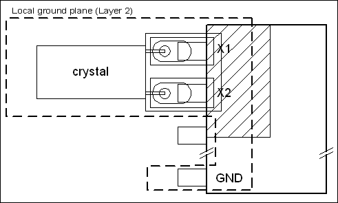
Figure 5. Recommended layout for crystal.
Checking For OscillationThe first impulse that a designer has when checking for oscillator operation often is to connect an oscilloscope probe to the oscillator input (X1) or output (X2) pin. Doing so is not recommended when using a Real-Time Clock. Since the oscillator is designed to run at low power (which extends operating time from a battery), loading the oscillator with an oscilloscope probe is likely to stop the oscillator. If the oscillator does not stop, the additional loading will reduce the signal amplitude, and may cause erratic operation, such as varying amplitude. Oscillation should therefore be verified indirectly.
Oscillation can be verified several ways. One method is to read the seconds register multiple times, looking for the data to increment. On RTCs with an OSF (Oscillator Stop Flag), clearing and then monitoring this bit will verify that the oscillator has started and is continuously running. These methods won't work if the designer is troubleshooting a design and cannot communicate with the RTC. An alternate method is to check the square wave output on RTCs that have a square wave output. Check the datasheet to verify if the RTC must be written first to enable the oscillator and square wave output. Note that most RTC square wave outputs are open-drain, and require a pull up resistor for operation. The square wave output can also be used to verify the accuracy of the RTC , however, a frequency counter with sufficient accuracy must be used.
Fast ClocksThe following are the most common scenarios that cause a crystal-based RTC to run fast. Noise coupling into the crystal from adjacent signals. This problem has been extensively covered above. Noise coupling usually causes an RTC to be grossly inaccurate. Wrong crystal. An RTC typically runs fast if a crystal with a specified load capacitance (CL) greater than the RTC-specified load capacitance is used. The severity of the inaccuracy is dependent on the value of the CL. For example, using a crystal with a CL of 12pF on an RTC designed with a 6pF CL causes the RTC to be about 3 to 4 minutes per month fast. Slow ClocksThe following are the most common scenarios that cause a crystal-based RTC to run slow. Overshoots on RTC input pins. It is possible to cause a RTC to run slow by periodically stopping the oscillator. This can be inadvertently accomplished by noisy input signals to the RTC. If an input signal rises to a voltage that is greater than a diode drop (~ 0.3V) above VDD , the ESD protection diode for the input pin will forward bias, allowing the substrate to be flooded with current. This, in turn, stops the oscillator until the input signal voltage decreases to below a diode drop above VDD.
This mechanism can cause the oscillator to stop frequently if input signals are noisy. Therefore, care should be taken to ensure there is no overshoot on input signals.
Another situation that is common to overshoot problem is having an input to the RTC at 5V when the RTC is in battery-backup mode. This can be a problem in systems that systematically shut down certain circuits but keep others powered up. It is very important to ensure there are no input signals to the RTC that are greater than the battery voltage (unless stated otherwise in the device data sheet) when the device is in battery-backup mode.
Wrong crystal. A RTC typically runs slow if a crystal with a specified CL is less than the CL of the RTC. The severity of the inaccuracy is dependent on the value of the CL. Stray capacitance. Stray capacitance between the crystal pins and / or to ground can slow an RTC down. Therefore, care must be taken when designing the PC board layout to ensure the stray capacitance is kept to a minimum. Temperature. The further the operating temperature is from the crystal turnover temperature, the slower the crystal oscillates . See Figures 3 and 4. Clock Does Not RunThe following are the most common scenarios that cause a RTC to not run. The single most common problem when the clock does not run is that the CH (clock halt) or EOSC (enable oscillator) bit has not been set or cleared, as required. Many Dallas RTCs include a circuit that keeps the oscillator from running when power is first applied. This allows a system to wait for shipment to the customer, without drawing power from the backup batte ry. When the system is powered for the first time, the software / firmware must enable the oscillator and prompt the user for the correct time and date. Surface mount crystals may have some NC (no connect) pins. Make sure that the correct pins from the crystal are connected to the X1 and X2 pins. Crystal Manufacturing Issues Tuning fork crystals should not be exposed to ultrasonic cleaning. They are susceptible to damage from resonant vibration.
Crystals should not be exposed to temperatures above their maximum ratings. Exposure to excessive temperatures may damage the crystal, and usually increase the ESR. Crystal "cans" should not be soldered to a PC board. This is sometimes done to ground the case of the crystal. Soldering directly to the case of the crystal usually subjects the unit to excessive temperatures.
RTCs should generally be used in noncondensing environments. Moisture forming around the oscillator conductors can cause leakage, which can cause the oscillator to stop. Conformal coatings can be used to protect the circuit, however, conformal coating may by itself cause problems.
Some conformal coatings, especially epoxy-based materials, can have unacceptable levels of ionic contamination. In addition, conformal coatings can, if the PC board surface is not sufficiently cleaned prior to conformal coating, cause contaminants to concentrate around leads and traces.
Solder flux residue can cause leakage between pins. RTC oscillator circuits are especially sensitive to leakage because of their low-power operation. Leakage between the oscillator input and output, or leakage to ground, often keep the oscillator from running.
References John R. Vig, Quartz Crystal Resonators and Oscillators for Frequency Control and Timing Applications, Advanced Crystal Technology, Fox Electronics, ECS, Inc. International,
Metal oxide semiconductor field effect (MOS) transistors can be divided into N-channel and P-channel. P-channel silicon MOS field-effect transistors have two P+ regions on the N-type silicon substrate, which are called source and The drain is not conductive between the two poles, and when a sufficient positive voltage (gate ground) is applied to the source, the surface of the N-type silicon under the gate exhibits a P-type inversion layer, which becomes a channel connecting the source and the drain. . Changing the gate voltage changes the density of the holes in the channel, thereby changing the resistance of the channel. Such a MOS Field Effect Transistor is called a P-channel enhancement type field effect transistor. If the surface of the N-type silicon substrate is free of gate voltage, the P-type inversion layer channel already exists, and the appropriate bias voltage can increase or decrease the resistance of the channel. Such a MOS field effect transistor is referred to as a P-channel depletion field effect transistor. They are collectively referred to as PMOS transistors.
P Channel Mosfet,P Channel Power Mosfet,Field Effect Transistor,Field Effect Transistor Symbol
Dongguan Agertech Technology Co., Ltd. , https://www.agertechcomponents.com