
Abstract: This applicaTIon note describes the JTAG hardware boundary scan chain for the DS26522 dual-port, single-chip transceiver. The DS26522 is composed of two dice, and the JTAG funcTIonality is the same as two separate devices daisy chained together. This applicaTIon note contains a complete breakdown of the JTAG scan chain and explains how to access all of the scan cells in the boundary.
OverviewThis applicaTIon note describes the JTAG hardware boundary scan chain for the DS26522 dual-port T1 / E1 / J1 single-chip transceiver (SCT). It is a dual-die module with two separate JTAG controllers in the same package (see Figure 1) . Notice the internal JTAG connections. The JTDI pin is connected to the JTDI input of the first die (port 1), while the JTDO pin is connected to the JTDO output of the second die (port 2). JTRST, JTCLK, and JTMS are wired together in parallel to both ports. This causes the DS26522 to appear as two separate devices in any JTAG software application. To solve this issue, two BSDL files have been created: one for port 1 and one for port 2.
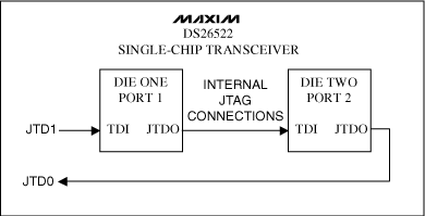
Figure 1. DS26522 JTAG Scan Chain
If the user would like to do any type of JTAG testing that requires a board netlist, the netlist will need to be modified to ensure that there are two unique instances of the DS26522 that correspond to the two BSDL files. Table 1 contains the port location (SCT port), the pin names, BSDL cell scan position, BSDL cell name and other useful information that correspond to the pins in each BSDL file. The table has been sorted by port location (SCT number) and then BSDL cell scan position. This should allow easy access to the necessary information about which BSDL cell scan position maps to which port location and BGA pin number. Incomplete or incorrect JTAG testing can be caused by the failure to modify the netlist accordingly.
Table 1. DS26522 JTAG scan chain: BGA pin to BSDL cell mapping
ConclusionThis application note explains in detail about the JTAG hardware boundary scan chain for the DS26522 (SCT). The DS26522 is composed of two die and the JTAG functionality is the same as two separate devices daisy chained together. The application note also contains a complete breakdown of the JTAG scan chain and explains how to access all of the boundary scan cells in the device.
If you have further questions about the DS26522 or our Telecom products at Maxim, please contact the Telecommunication Applications support team through email at var name = "Telecom.Support @"; var domain = "maxim-ic.com"; document.write ( "" + name + domain + ""); Telecom. or call 972-371-6555.
OverviewThis applicaTIon note describes the JTAG hardware boundary scan chain for the DS26522 dual-port T1 / E1 / J1 single-chip transceiver (SCT). It is a dual-die module with two separate JTAG controllers in the same package (see Figure 1) . Notice the internal JTAG connections. The JTDI pin is connected to the JTDI input of the first die (port 1), while the JTDO pin is connected to the JTDO output of the second die (port 2). JTRST, JTCLK, and JTMS are wired together in parallel to both ports. This causes the DS26522 to appear as two separate devices in any JTAG software application. To solve this issue, two BSDL files have been created: one for port 1 and one for port 2.
Figure 1. DS26522 JTAG Scan Chain
If the user would like to do any type of JTAG testing that requires a board netlist, the netlist will need to be modified to ensure that there are two unique instances of the DS26522 that correspond to the two BSDL files. Table 1 contains the port location (SCT port), the pin names, BSDL cell scan position, BSDL cell name and other useful information that correspond to the pins in each BSDL file. The table has been sorted by port location (SCT number) and then BSDL cell scan position. This should allow easy access to the necessary information about which BSDL cell scan position maps to which port location and BGA pin number. Incomplete or incorrect JTAG testing can be caused by the failure to modify the netlist accordingly.
Table 1. DS26522 JTAG scan chain: BGA pin to BSDL cell mapping
| SCT Port | BGA Pin | BSDL Scan Position | BSDL Scan Name | BSDL Scan Function | Data Sheet Symbol | Data Sheet Description |
| 1 | F8 | 0 | TSER | Observe_only | TSER1 | Transmit NRZ Serial Data |
| 1 | G8 | 1 | TCLK | Observe_only | TCLK1 | Transmit Clock |
| 1 | H8 | 2 | TSYSCLK | Observe_only | TSYSCLK1 | Transmit System Clock |
| 1 | - | 3 | - | Control | - | - |
| 1 | J7 | 4 | TSYNC | Output3 | TSYNC1 | Transmit Synchronization |
| 1 | - | 5 | TSYNC | Observe_only | - | - |
| 1 | - | 6 | - | Control | - | - |
| 1 | G7 | 7 | TSSYNCIO | Output3 | TSSYNCIO1 | Transmit System Synchronization In or Out |
| 1 | - | 8 | TSSYNCIO | Observe_only | - | - |
| 1 | - | 9 | - | Control | - | - |
| 1 | H7 | 10 | TSIG | Output3 | TSIG1 | Transmit Signaling |
| 1 | - | 11 | TSIG | Observe_only | - | - |
| 1 | - | 12 | - | Control | - | - |
| 1 | F7 | 13 | TCHBLK_CLK | Output3 | TCHBLK / CLK1 | Transmit Channel Block or Transmit Channel Block Clock |
| 1 | - | 14 | TCHBLK_CLK | Observe_only | - | - |
| 1 | - | 15 | - | Control | - | - |
| 1 | K5 | 16 | RSER | Output3 | RSER1 | Received Serial Data |
| 1 | - | 17 | - | Control | - | - |
| 1 | L8 | 18 | RCLK | Output3 | RCLK1 | Receive Clock |
| 1 | - | 19 | RCLK | Observe_only | - | - |
| 1 | J8 | 20 | RSYSCLK | Observe_only | RSYSCLK1 | Receive System Clock |
| 1 | - | twenty one | - | Control | - | - |
| 1 | K7 | twenty two | RYSNC | Output3 | RSYNC1 | Receive Synchronization |
| 1 | - | twenty three | RYSNC | Observe_only | - | - |
| 1 | - | twenty four | - | Control | - | - |
| 1 | G6 | 25 | RM_RFSYNC | Output3 | RM / RFSYNC1 | Receive Multiframe or Frame Synchronization |
| 1 | - | 26 | RM_RFSYNC | Observe_only | - | - |
| 1 | - | 27 | - | Control | - | - |
| 1 | H6 | 28 | RSIG | Output3 | RSIG1 | Receive Signaling |
| 1 | - | 29 | RSIG | Observe_only | - | - |
| 1 | - | 30 | - | Control | - | - |
| 1 | F6 | 31 | AL_RSIGF_FLOS | Output3 | AL / RSIGF / FLOS1 | Analog Loss or Receive Signaling Freeze or Framer LOS |
| 1 | - | 32 | - | Control | - | - |
| 1 | J5 | 33 | RLF_LTC | Output3 | RLF / LTC1 | Receive Loss of Frame or Loss of Transmit Clock |
| 1 | - | 34 | - | Control | - | - |
| 1 | J6 | 35 | RCHBLK_CLK | Output3 | RCHBLK / CLK1 | Receive Channel Block or Receive Channel Block Clock |
| 1 | - | 36 | RCHBLK_CLK | Observe_only | - | - |
| 1 | - | 37 | - | Control | - | - |
| 1 | K6 | 38 | BPCLK | Output3 | BPCLK1 | Backplane Clock |
| 1 | - | 39 | - | Control | - | - |
| 1 | K8 | 40 | REFCLKIO | Output3 | REFCLKIO1 | Reference Clock Input or Output |
| 1 | - | 41 | REFCLKIO | Observe_only | - | - |
| 1 | M9 | 42 | MCLK | Observe_only | MCLK | Master Clock |
| 1 | K3 | 43 | RESETB | Observe_only | RESETB | Reset Bar |
| 1 | - | 44 | - | Control | - | - |
| 1 | K4 | 45 | INTB | Output3 | INTB | Interrupt Bar |
| 1 | J3 | 46 | WRB_RWB | Observe_only | WRB / RWB | Write Bar or Read-Write Bar |
| 1 | H3 | 47 | RDB_DSB | Observe_only | RDB / DSB | Read Data Bar or Strobe Bar |
| 1 | L4 | 48 | CSB | Observe_only | CSB1 | Chip Select Bar |
| 1 | - | 49 | - | Control | - | - |
| 1 | M3 | 50 | D0 | Output3 | D0 / SPI_MISO | Data [0] or SPI Serial Interface Data Master-In Slave-Out |
| 1 | - | 51 | D0 | Observe_only | - | - |
| 1 | - | 52 | - | Control | - | - |
| 1 | L3 | 53 | D1 | Output3 | D1 / SPI_MOSI | Data [1] or SPI Serial Interface Data Master-Out Slave-In |
| 1 | - | 54 | D1 | Observe_only | - | - |
| 1 | - | 55 | - | Control | - | - |
| 1 | M2 | 56 | D2 | Output3 | D [2] / SPI_SCLK | Data [2] or SPI Serial Interface Clock |
| 1 | - | 57 | D2 | Observe_only | - | - |
| 1 | - | 58 | - | Control | - | - |
| 1 | M1 | 59 | D3 | Output3 | D [3] | Data [3] |
| 1 | - | 60 | D3 | Observe_only | - | - |
| 1 | - | 61 | - | Control | - | - |
| 1 | L2 | 62 | D4 | Output3 | D [4] | Data [4] |
| 1 | - | 63 | D4 | Observe_only | - | - |
| 1 | - | 64 | - | Control | - | - |
| 1 | L1 | 65 | D5 | Output3 | D [5] / SPI_SWAP | Data [5] or SPI Bit Order Swap |
| 1 | - | 66 | D5 | Observe_only | - | - |
| 1 | - | 67 | - | Control | - | - |
| 1 | K2 | 68 | D6 | Output3 | D [6] / SPI_CPHA | Data [6] or SPI Interface Clock Phase |
| 1 | - | 69 | D6 | Observe_only | - | - |
| 1 | - | 70 | - | Control | - | - |
| 1 | K1 | 71 | D7 | Output3 | D [7] / SPI_CPOL | Data [7] or SPI Interface Clock Polarity |
| 1 | - | 72 | D7 | Observe_only | - | - |
| 1 | J2 | 73 | A0 | Observe_only | A0 | Address [0] |
| 1 | J1 | 74 | A1 | Observe_only | A1 | Address [1] |
| 1 | H2 | 75 | A2 | Observe_only | A2 | Address [2] |
| 1 | H1 | 76 | A3 | Observe_only | A3 | Address [3] |
| 1 | G2 | 77 | A4 | Observe_only | A4 | Address [4] |
| 1 | G1 | 78 | A5 | Observe_only | A5 | Address [5] |
| 1 | F2 | 79 | A6 | Observe_only | A6 | Address [6] |
| 1 | F1 | 80 | A7 | Observe_only | A7 | Address [7] |
| 1 | E2 | 81 | A8 | Observe_only | A8 | Address [8] |
| 1 | E1 | 82 | A12 | Observe_only | A12 | Address [12] |
| 1 | E6 | 83 | TXEN_B | Observe_only | TXENABLE1 | Transmit Enable |
| 1 | E5 | 84 | BTS | Observe_only | BTS | Bus Type Select |
| 1 | D7 | 85 | SPI_SEL | Observe_only | SPI_SEL | SPI Serial Bus Mode Select |
| 2 | E12 | 0 | TSER | Observe_only | TSER2 | Transmit NRZ Serial Data |
| 2 | G11 | 1 | TCLK | Observe_only | TCLK2 | Transmit Clock |
| 2 | H11 | 2 | TSYSCLK | Observe_only | TSYSCLK2 | Transmit System Clock |
| 2 | - | 3 | - | Control | - | - |
| 2 | F11 | 4 | TSYNC | Output3 | TSYNC2 | Transmit Synchronization |
| 2 | - | 5 | TSYNC | Observe_only | - | - |
| 2 | - | 6 | - | Control | - | - |
| 2 | F12 | 7 | TSSYNCIO | Output3 | TSSYNCIO2 | Transmit System Synchronization In / Out |
| 2 | - | 8 | TSSYNCIO | Observe_only | - | - |
| 2 | - | 9 | - | Control | - | - |
| 2 | E11 | 10 | TSIG | Output3 | TSIG2 | Transmit Signaling |
| 2 | - | 11 | TSIG | Observe_only | - | - |
| 2 | - | 12 | - | Control | - | - |
| 2 | G12 | 13 | TCHBLK_CLK | Output3 | TCHBLK / CLK2 | Transmit Channel Block or Transmit Channel Block Clock |
| 2 | - | 14 | TCHBLK_CLK | Observe_only | - | - |
| 2 | - | 15 | - | Control | - | - |
| 2 | H12 | 16 | RSER | Output3 | RSER2 | Received Serial Data |
| 2 | - | 17 | - | Control | - | - |
| 2 | L9 | 18 | RCLK | Output3 | RCLK2 | Receive Clock |
| 2 | - | 19 | RCLK | Observe_only | - | - |
| 2 | J11 | 20 | RSYSCLK | Observe_only | RSYSCLK2 | Receive System Clock |
| 2 | - | twenty one | - | Control | - | - |
| 2 | K12 | twenty two | RYSNC | Output3 | RSYNC2 | Receive Synchronization |
| 2 | - | twenty three | RYSNC | Observe_only | - | - |
| 2 | - | twenty four | - | Control | - | - |
| 2 | L12 | 25 | RM_RFSYNC | Output3 | RM / RFSYNC2 | Receive Multiframe or Frame Synchronization |
| 2 | - | 26 | RM_RFSYNC | Observe_only | - | - |
| 2 | - | 27 | - | Control | - | - |
| 2 | L11 | 28 | RSIG | Output3 | RSIG2 | Receive Signaling |
| 2 | - | 29 | RSIG | Observe_only | - | - |
| 2 | - | 30 | - | Control | - | - |
| 2 | J12 | 31 | AL_RSIGF_FLOS | Output3 | AL / RSIGF / FLOS2 | Analog Loss or Receive Signaling Freeze or Framer LOS |
| 2 | - | 32 | - | Control | - | - |
| 2 | M12 | 33 | RLF_LTC | Output3 | RLF / LTC2 | Receive Loss of Frame or Loss of Transmit Clock |
| 2 | - | 34 | - | Control | - | - |
| 2 | M11 | 35 | RCHBLK_CLK | Output3 | RCHBLK / CLK2 | Receive Channel Block or Receive Channel Block Clock |
| 2 | - | 36 | RCHBLK_CLK | Observe_only | - | - |
| 2 | - | 37 | - | Control | - | - |
| 2 | M10 | 38 | BPCLK | Output3 | BPCLK2 | Backplane Clock |
| 2 | - | 39 | - | Control | - | - |
| 2 | L10 | 40 | REFCLKIO | Output3 | REFCLKIO2 | Reference Clock Input or Output |
| 2 | - | 41 | REFCLKIO | Observe_only | - | - |
| 2 | M9 | 42 | MCLK | Observe_only | MCLK | Master Clock |
| 2 | K3 | 43 | RESETB | Observe_only | RESETB | Reset Bar |
| 2 | - | 44 | - | Control | - | - |
| 2 | K4 | 45 | INTB | Output3 | INTB | Interrupt Bar |
| 2 | J3 | 46 | WRB_RWB | Observe_only | WRB / RWB | Write Bar or Read-Write Bar |
| 2 | H3 | 47 | RDB_DSB | Observe_only | RDB / DSB | Read Data Bar or Strobe Bar |
| 2 | M4 | 48 | CSB | Observe_only | CSB2 | Chip Select Bar |
| 2 | - | 49 | - | Control | - | - |
| 2 | M3 | 50 | D0 | Output3 | D [0] / SPI_MISO | Data [0] or SPI Serial Interface Data Master-In Slave-Out |
| 2 | - | 51 | D0 | Observe_only | - | - |
| 2 | - | 52 | - | Control | - | - |
| 2 | L3 | 53 | D1 | Output3 | D [1] / SPI_MOSI | Data [1] or SPI Serial Interface Data Master-Out Slave-In |
| 2 | - | 54 | D1 | Observe_only | - | - |
| 2 | - | 55 | - | Control | - | - |
| 2 | M2 | 56 | D2 | Output3 | D [2] / SPI_SCLK | Data [2] or SPI Serial Interface Clock |
| 2 | - | 57 | D2 | Observe_only | - | - |
| 2 | - | 58 | - | Control | - | - |
| 2 | M1 | 59 | D3 | Output3 | D [3] | Data [3] |
| 2 | - | 60 | D3 | Observe_only | - | - |
| 2 | - | 61 | - | Control | - | - |
| 2 | L2 | 62 | D4 | Output3 | D [4] | Data [4] |
| 2 | - | 63 | D4 | Observe_only | - | - |
| 2 | - | 64 | - | Control | - | - |
| 2 | L1 | 65 | D5 | Output3 | D [5] / SPI_SWAP | Data [5] or SPI Bit Order Swap |
| 2 | - | 66 | D5 | Observe_only | - | - |
| 2 | - | 67 | - | Control | - | - |
| 2 | K2 | 68 | D6 | Output3 | D [6] / SPI_CPHA | Data [6] or SPI Interface Clock Phase |
| 2 | - | 69 | D6 | Observe_only | - | - |
| 2 | - | 70 | - | Control | - | - |
| 2 | K1 | 71 | D7 | Output3 | D [7] / SPI_CPOL | Data [7] or SPI Interface Clock Polarity |
| 2 | - | 72 | D7 | Observe_only | - | - |
| 2 | J2 | 73 | A0 | Observe_only | A0 | Address [0] |
| 2 | J1 | 74 | A1 | Observe_only | A1 | Address [2] |
| 2 | H2 | 75 | A2 | Observe_only | A2 | Address [2] |
| 2 | H1 | 76 | A3 | Observe_only | A3 | Address [3] |
| 2 | G2 | 77 | A4 | Observe_only | A4 | Address [4] |
| 2 | G1 | 78 | A5 | Observe_only | A5 | Address [5] |
| 2 | F2 | 79 | A6 | Observe_only | A6 | Address [6] |
| 2 | F1 | 80 | A7 | Observe_only | A7 | Address [7] |
| 2 | E2 | 81 | A8 | Observe_only | A8 | Address [8] |
| 2 | E1 | 82 | A12 | Observe_only | A12 | Address [12] |
| 2 | E7 | 83 | TXEN_B | Observe_only | TXENABLE2 | Transmit Enable |
| 2 | E5 | 84 | BTS | Observe_only | BTS | Bus Type Select |
| 2 | D7 | 85 | SPI_SEL | Observe_only | SPI_SEL | SPI Serial Bus Mode Select |
If you have further questions about the DS26522 or our Telecom products at Maxim, please contact the Telecommunication Applications support team through email at var name = "Telecom.Support @"; var domain = "maxim-ic.com"; document.write ( "" + name + domain + ""); Telecom. or call 972-371-6555.
Dual Channel Brushless Dc Motor Controller
Dc Controller,Dc Speed Controller,Brushless Dc Controller,Dual Channel Brushless Dc Motor Controller
Jinan Keya Electron Science And Technology Co., Ltd. , https://www.keyaservo.com