
How do semiconductor manufacturers do the factory test of the chip? This is a necessary part of the chip after the film is released or before the market.
There are tens of thousands of chips in the daily flow of large companies, and the pressure of testing is very large. When the chip is made by the fab, it will enter the WaferTest phase. Testing at this stage may be performed at the fab or may be sent to a nearby test vendor agent. The production engineer will use the automatic test instrument (ATE) to run the program given by the chip designer, and roughly divide the chip into good/bad parts. The bad ones will be directly discarded. If there are too many bad films at this stage, the basic will It is believed that the fab's own yield is low. If the yield is below a certain value, the fab needs to lose money.
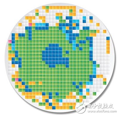
The test results of WT are often represented by such a graph:
After passing WaferTest, the wafer will be cut. The cut chips are sorted according to the previous results. Only good chips will be sent to the package factory. The location of the package is generally near the fab, because unpackaged chips cannot be transported over long distances. The type of package depends on the needs of the customer, some require a spherical BGA, and some require a pin. In short, this step is simple and has fewer faults. Since the success rate of the package is much larger than the production yield of the chip, it will not be tested after packaging.
After packaging, the chip will be sent to the test factories of major companies, also known as production plants. And carry out FinalTest. There are actually more than a dozen processes in the production plant, and FinalTest is just the first step. After FinalTest, you also need to sort, engrave, check the package, package and other steps. Then you can ship to the market.
FinalTest is the focus of the plant and requires a lot of mechanical and automation equipment. Its purpose is to rigorously classify chips. Take Intel's processor as an example. These phenomena may occur in FinalTest:
1. Although the WaferTest is passed, the chip is still bad.
2. The package is damaged.
3. The chip is partially damaged. For example, the CPU has 2 core damages, or the GPU is damaged, or the display interface is damaged.
4. The chip is good and there is no fault
At this point, the engineer needs to work with the marketing department to decide how to classify the chips. For example, if the GPU is broken, it can be used as a "Celelian" series processor without a display core. If the CPU is broken 2, it can be used as a "Core i3" series processor. The chip works fine, but the working frequency is not high, it can be used as the "Core i5" series processor. No problem at all, can be a "Core i7" processor.
(The above paragraph is only a simplification of the process of "the result of the chip test affects the final label of the product", not to say that Intel's chip production pipeline is as described above. In fact, Intel maintains multiple product lines at the same time. The chips for i3 and i7 are not on the same line.)
What should I do with FinalTest here?
For example, the processor can be divided into two steps: 1. Automatic Test Equipment (ATE). 2. System Level Test (SLT). No. 2 is a necessary item. No. 1 general small company can not afford.
ATE testing typically takes a few seconds, while SLT takes a few hours. The existence of ATE greatly reduces the chip test time.
ATE is responsible for a lot of projects and has a strong logical relevance. The tests must be performed in order, and the test items in the following columns may be skipped for the results of the preceding test. The content of these projects is company secret, I only list a few: such as power detection, pin DC detection, test logic (generally JTAG) detection, burn-in, physical connection PHY detection, IP internal detection (including Scan, BIST, FuncTIon, etc., IP IO detection (such as DDR, SATA, PLL, PCIE, Display, etc.), auxiliary function detection (such as thermodynamic characteristics, fuse, etc.).
These test items will give Pass/Fail. It is the test engineer's job to analyze the physique of the chip based on these Pass/Fail.
The SLT is logically simpler. Install the chip on the motherboard, configure the memory, peripherals, boot an operating system, then test it with a software bake, record the results and compare. Also check BIOS related items.

The picture shows the layout of the test plant
All of this work requires the chip design engineer to design before the tape is released. The test work is carried out by the dedicated circuit in the chip. The construction of this part of the circuit is done by the DFT engineer. After the film is released, the DFT engineer also generates the matching input vector, which usually generates tens of thousands. Whether these vectors can properly detect the function of the chip requires a product development engineer to guarantee. In addition, test engineers, product engineers, and assistants are required to ensure that the production tasks of tens of thousands of chips per day are not delayed due to test logic bugs.
Considering that each test version iteration is a code of several hundred thousand lines, the code can not be mistaken. Test engineers who need hundreds of people work together. This is not a line-up mechanic, so testing is a time-consuming and laborious task. In fact, the testing costs of many large company chips are close to the cost of research and development.
1. Why do you want to test the chip?
The complexity of the chip is getting higher and higher. In order to ensure that there is no problem with the factory chip, it needs to be tested before leaving the factory to ensure functional integrity. As a large-scale production of chips, large-scale automated testing is the only solution. It is impossible to accomplish such tasks by manual or benchtest.
2. In what part of the chip test?
Chip testing is actually a relatively large category. It is generally divided into wafertest and finaltest from the object of testing. The objects are chips that have not been packaged, and chips that have already been packaged. Why do you want to divide it into two paragraphs? To put it simply, because the package is also cost-effective, in order to save the cost as much as possible, some tests may be performed before the chip package to eliminate some broken chips. In order to ensure that the chip is no problem, finaltest, that is, FT test is the last interception, it is also a necessary link.
3. How to test the chip?
This requires a professional ATE, also known as automaTIctestequipment. Take finaltest as an example. First, select the appropriate ATE machine according to the type of chip, such as automoTIve, MixedSignal, memory, etc. On this basis, according to the test requirements of the chip, (there may be a special testspecificaTIon documentation, or simply let the test engineer design the testspec according to the datasheet), do a complete testplan. On this basis, design a peripheral circuit loadboard, generally we call it DIBorPIBorHIB, to connect the instrument of the ATE machine and the chip itself. At the same time, it is necessary to carry out test program development, according to each test item, to program, manipulate the instrument to connect to the pin of the chip, give specific excitation conditions, and then capture the reaction of the chip pin, for example, give an electrical signal, which can be specific The current, voltage, or voltage waveform is then captured to capture its response. According to the result, it is determined that this test item is pass or fail. After a series of test items, whether the chip is good or not, there is a result. A good chip will be placed in a specific place, and it is not good to put it in a different place according to the test type of the fail.
Therefore, in the question of the landlord, for the testing of various functions, it may indeed be necessary to write code one by one to do test development, which is also a large part of my daily work.
The chip fail can be as follows:
1. Function fail, a function point is not realized, which is often caused by design, usually by simulation before the design phase to verify the function to ensure, so usually design a chip, simulation verification will take about 80% of the time
2. Performance fail, a performance indicator requires no clearance, such as 2G cpu can only run to 1.5G, digital-to-analog converter under the required conversion speed and bandwidth conditions, the effective number of eeno to reach 12, but only 10 Bit, and lna's noise figure indicator is not up to standard and so on. This kind of problem is usually caused by two problems. One is that there is not enough space in the design of the system in the early stage, and the other is that the physical implementation layout is too bad. This type of problem is usually verified by post-simulation.
3. The resulting fail. The reason for this problem is to mention the production of monocrystalline silicon. Those who have studied semiconductor physics know that monocrystalline silicon is a regular face-centered cubic structure. It has several crystal orientations. Usually, we grow single crystals by pulling in the 111 crystal orientation. However, due to various external factors, such as temperature, pulling speed, and various randomness of quantum mechanics, misalignment occurs during growth, which is called defect. Another cause of defect generation is the irregular structure that is caused by ion implantation, even if it is not annealed. These problems in the semiconductor can lead to device failure, which in turn affects the entire chip. Therefore, in order to produce a failed or semi-failed chip after production, special test circuits will be added at the time of design, such as testmux in the simulation, scan chain in the number, mbist, and boundry scan. (Measure io and binding) to ensure that the ok chip is delivered to the customer. Products that fail or are semi-failed are either discarded or sold as low-end products after castration. This is called the dft test. Usually the dft test will be tested before or after the package according to requirements. There is a special ate test machine in the factory, and the probe is used to connect the test io for dft test. Usually the dft test does not test the function, because the goods are collected according to time. The more concise and effective the test case is, the better. And the use case is too complicated, it will affect the shipping speed, such as 100w of goods, one chip test for one second, single dft test for 24 hours does not stop more than 11 days.
4. What types of tests are included in the general chip test?
In general, including pin connectivity testing, leakage current testing, some DC (directcurrent) testing, functional testing (functionaltest), Trimtest, there are some other tests depending on the chip type, such as AD/DA will have some special Test type.
The purpose of the chip test is to find the chip that is not problematic while saving the cost as much as possible. Therefore, the type of defect that is easy to detect or relatively common will be detected first. In general, the first thing we will do is connectivity testing, which we call continuitytest. This is to check if the connectivity of each pin is normal.
Product Description
SPD Surge Protective Device,Lightning Surge Protector
Surge Protection Device (SPD)
It is a device used to limiting instant surge voltage and discharge surge current, it at least including a non-linear component.
Surge protective Device Model Selection
With the impact of international information flow, the rapid development of microelectronic science and technology, communication, computer and automatic control technology, make the building start to go for high quality, high functional area, formed a new building style-intelligent building. As inside the intelligent building there are lot of information system, <<Building lightning protection design norm>> GB50057-94(2002 vision)(hereafter brief as <<lightning protection norm>>) put forward the relative requirement to install the surge protective device, to ensure the information system safely and stable running.
SPD essentially is a equipotential connection material, its model selection is according to the different lightning protection area, different lightning electromagnetic pulse critical and different equipotential connection position, decide which kind of SPD used in the area, to achieve the equipotential connection with the common earth electrode. Our statement will based on SPD's maximum discharge current Imax, continuous operating voltage Uc, protection voltage Up, alarm mode etc.
As per << Lightning Protection Norm>> item 6.4.4 stipulation "SPD must can withstand the expected lightning current flow and should confirm to the additional two requirements: the maximum clamp voltage during surge across, capable to extinguish the power frequency follow-on current after lightning current across." That is the value of SPD's max. clamp voltage add its induction voltage of two ends should be same with the system's basic insulation level and the equipment allowed max. surge voltage.
SPD for Power Supply System Series Selection Guide
The installation of SPD at each lightning protection zone, according to the standard of low voltage electrical appearance, make classification of electrical equipment in accordance with the over voltage category, its insulation withstand impulse voltage level can determine the selection of SPD. According to the standard of low voltage electrical appearance, make classification of electrical equipment in accordance with the over voltage category as signal level, loading level, distribution and control level, power supply level. Its insulation withstand impulse voltage level are:1500V,2500V,4000V,6000V. As per to the protected equipment installation position different and the different lightning current of different lightning protection zone, to determine the installation position of SPD for power supply and the break-over capacity.
The installation distance between each level SPD should not more than 10m, the distance between SPD and protected equipment should as short as possible, not more than 10m. If due to limitation of installation position, can't guarantee the installation distance, then need to install decoupling component between each level SPD, make the after class SPD can be protected by the prior class SPD. In the low voltage power supply system, connecting an inductor can achieve the decoupling purpose.
SPD for power supply system specification selection principle
Max. continuous operating voltage: bigger than protected equipment, the system's max. continuous operating voltage.
TT System: Uc≥1.55Uo (Uo is low voltage system to null line voltage)
TN System: Uc≥1.15Uo
IT System: Uc≥1.15Uo(Uo is low voltage system to line voltage)
Voltage Protection Level: less than the insulation withstand impulse voltage of protected equipment
Rated discharge current: determined as per to the lightning situation of the position installed and lightning protection zone.
SP1 Series
Normal Working Conditions
-Altitude not exceed 2000m
-Ambient air temperature:
Normal range: -5ºC~+40ºC
Extend range: -40ºC~+80ºC
-Relative Humidity: 30% - 90% under indoor temperature condition
- At the place without obviously shaking and shock vibration
- Non-explosion danger medium, non-corrosion gas and dust ( including conductive dust)
Classification
-As per Nominal Discharge Current:
5,10,20,30,40,60KA(8/20µs)
- As per Maximum continuous operating voltage:
275V,320V,385V,420V,440V,460V
- As per to poles
1P,1P+N,2P,3P,3P+N,4P
- As per auxiliary functions:
a. With remote signal output ( remote alarm function)
b. Without remote signal output
Selection Principle
- The continuous applied voltage on the two terminals of SPD should not more than the maximum continuous operating voltage Uc value;
- The voltage protection level Up of SPD should less than the maximum impulse withstand voltage of the protected equipment;
- As per to the different earthing system and protection mode to select the specification accordingly;
Product Features
1, built-in over-current overheating, temperature control circuit technology.
2, the module design, easy installation, online replacement.
3, low leakage current, fast response time, low residual voltage.
4, alarm indication device, green (normal) v red (fault).
| Model/Technical Parameters | WR-B60 | WR-B80 | WR-B100 | WR-B120 | WR-B150 |
| Rated Operating Voltage Un (V ~) | 220V 380V | 220V 380V | 220V 380V | 220V 380V | 220V 380V |
| Maximum Continuous Operating Voltage Uc (V ~) kV | 385V 420V | 385V 420V | 385V 420V | 385V 420V | 385V 420V |
| Voltage Protection Level Up (V ~) kV | ≤1.8≤2.2 | ≤2.4≤2.5 | ≤2.5≤3.2 | ≤3.4≤3.7 | ≤4.0≤4.5 |
|
Maximum Discharge Current Imax(8/μ20μs)kA |
60 | 80 | 100 | 120 | 150 |
|
Nominal Discharge Current In(8/μ20μs)kA |
30 | 40 | 60 | 80 | 100 |
| Response Time | <25 | <100 | |||
| L/N(mm²)The Cross Section Of L/N Line | 16,25 | 16,25 | 16,25 | 16,25 | 25,35 |
| PE (mm²)The Cross Section Of PE Line | 16,25 | 25,35 | 25,35 | 25,35 | 35 |
| Fuse or Switch (A) | 63A | 63A | 63A,100A | 63A,100A | 63A,125A |
| The Line Section of Communication and Alarm (mm²) | ≥ 1.5 | ||||
|
Operating Environment-C |
(-40ºC~-+85ºC) | ||||
| Relative humidity 25 ºC | ≤95% | ||||
| installation | Standard Rail35mm | ||||
| Material of Outer Covering | Fiber Glass Reinforced Plastic | ||||
Surge Protector SPD,Surge Protection Device SPD,SPD
Wenzhou Korlen Electric Appliances Co., Ltd. , https://www.zjmotorstarter.com