
1. Pkg and PCB System
As the demand for data processing and computing continues to rise, the core of electronic devices—chip process size—is becoming smaller and smaller, while their operating frequency is increasing significantly. Modern processors now operate at GHz frequencies, and digital signals have shorter rise and fall times, leading to higher harmonic components. This makes digital systems high-frequency and high-bandwidth in nature. For a fully assembled PCB, both the PCB itself and the package (Pkg) can resonate within this frequency range. If the power delivery system (PDS) is not designed properly, structural resonance may occur, degrading power quality and potentially causing system failures.
In addition, with increased component density, systems often adopt low voltage and low swing designs to reduce power consumption. However, low-voltage signals are more susceptible to noise interference. Common noise sources include coupling, crosstalk, and electromagnetic interference (EMI), but the most significant issue comes from power supply noise, particularly Simultaneous Switching Noise (SSN).
The entire PDS system includes not only the circuit system but also an electromagnetic field formed by the power source and ground plane. The figure below shows a schematic of a typical power delivery system.
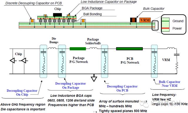
Figure 1: Schematic of a Typical Power Delivery System
2. Measurement of Pkg and PCB Systems
When discussing ground bounce noise (GBN), it's common to focus only on the PCB and measure its S parameter |S21| as a reference for GBN magnitude. Port 1 represents the SSN excitation source, typically located at the active IC on the PCB. A lower |S21| indicates better PDS design and reduced GBN. However, noise originates from the IC, travels through the Pkg power system, and then moves via the package’s vias and solder balls to the PCB power system (see Figure 1). Therefore, it’s essential to consider both the Pkg and PCB together to accurately describe GBN behavior in high-speed digital systems.
To address this, we designed a PDS structure (Figure 2) that represents the Pkg power system mounted on the PCB.
 Figure 2: Schematic and Cross Section of BGA Package Mounted on PCB
The S parameters of this structure were measured using a network analyzer (HP8510C) and a probe station (Microtech) from 50 MHz to 5 GHz. Two 450 µm pitch GS probes were used, connected to the power ring and ground ring of the Pkg signal layer. The measurement setup is shown in Figure 3.
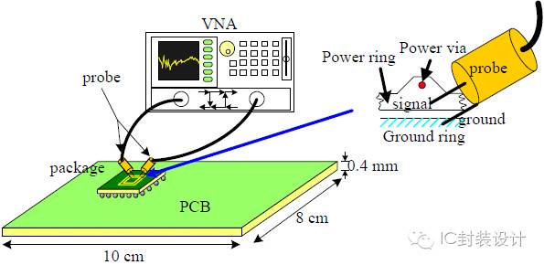
Figure 3: Structural Measurement Setup of BGA Package on PCB
The results of the Pkg+PCB structure’s S parameters are shown in Figure 4. We also conducted measurements for single Pkg and PCB structures for comparison to understand the differences between the full PDS system and individual components.
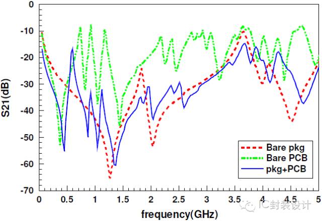
Figure 4: Measurement Results of BGA Package on PCB
From the results in Figure 4, we see that the GBN behavior varies significantly among the three structures. For a single Pkg, the S-parameter behaves like a capacitor below 1.3 GHz, but exhibits a resonant mode above 1.5 GHz. For a single PCB, there are resonant modes starting at 0.5 GHz, such as 0.73 GHz (TM01), 0.92 GHz (TM10), and 1.17 GHz (TM11), resulting in worse GBN performance than the single Pkg. When combining Pkg and PCB, before 1.5 GHz, there are three additional resonance points compared to the single Pkg. These resonances come from the PCB and couple into the Pkg power system through solder balls and vias, making the Pkg IC more vulnerable to noise. This highlights the importance of considering both Pkg and PCB together.
3. Effect of Decoupling Capacitors on Power Supply Noise
Traditionally, power plane noise is suppressed using decoupling capacitors. Many studies have been conducted on their use, but the size, placement, and number of capacitors are usually based on empirical rules.
Ideal Placement of Decoupling Capacitors
To study the impact of decoupling capacitor placement on the PDS, we used the Pkg+PCB structure, adding decoupling capacitors on the Pkg, on the PCB, or both. We measured the ideal placement by observing |S21|.
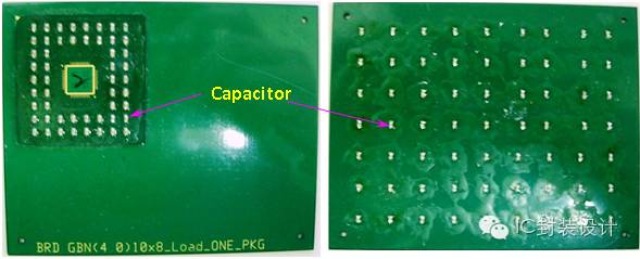
Figure 5: Decoupling Capacitors on Pkg and PCB
As shown in Figure 5, we tested three scenarios: placing 52 capacitors on the Pkg, 63 on the PCB, and 52 and 63 on both. Each had a capacitance of 100 nF, ESR of 0.04 Ω, and ESL of 0.63 nH. The results are shown in Figure 6.
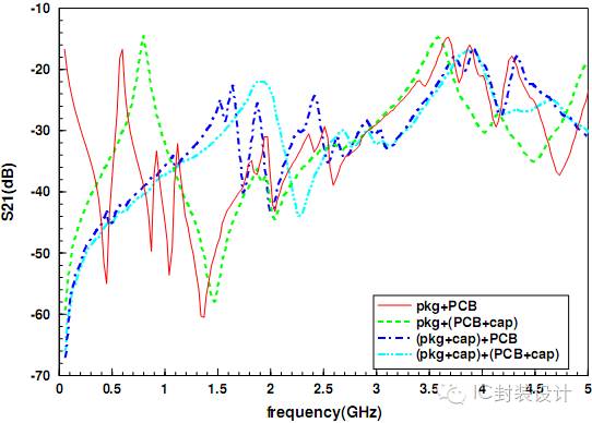 Figure 6: |S21| Comparison with Decoupling Capacitors at Different Positions
First, we divided the low frequency range up to 5 GHz into three parts. From 0 to 500 MHz, adding capacitors to either the Pkg or PCB significantly reduces the structure impedance and suppresses GBN. Second, from 0.5 GHz to 2 GHz, placing capacitors on both Pkg and PCB gives similar noise suppression. However, if only the PCB has capacitors, an extra resonance point near 800 MHz appears, which is worse than no capacitor. Thus, we must be cautious when adding capacitors to the PCB. Third, from 2 GHz to 5 GHz, the capacitors become less effective due to exceeding their own resonant frequency. The ESL causes the coupling capacitor to increase with frequency, gradually losing its ability to suppress high-frequency noise.
Effect of Decoupling Capacitor ESR
On the Pkg+PCB structure, we placed 12 decoupling capacitors and varied the ESR. The simulation results are shown in Figure 7. As ESR increases, the pole becomes flatter, and the zero point fills in, resulting in a relatively flat |S21| curve.
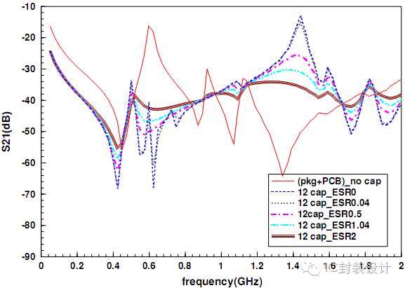 Figure 7: Effect of ESR on |S21|
Effect of Decoupling Capacitor ESL
On the same Pkg+PCB structure, we placed 12 decoupling capacitors and varied the ESL. The results are shown in Figure 8. As ESL increases, the amplitude of the resonance peak rises, and the resonance shifts toward lower frequencies, reducing noise suppression capability.
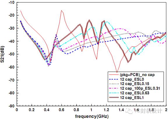 Figure 8: Effect of ESL on |S21|
Effect of Number of Decoupling Capacitors
Based on previous results, placing capacitors on the Pkg is more effective. So we focused on the number of capacitors on the Pkg. The placement of capacitors on the Pkg is shown in Figure 9, and the simulation result is shown in Figure 10.
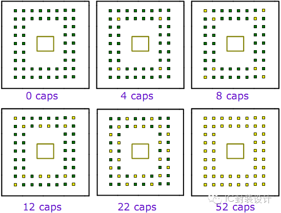 Figure 9: Capacitor Location on the Package
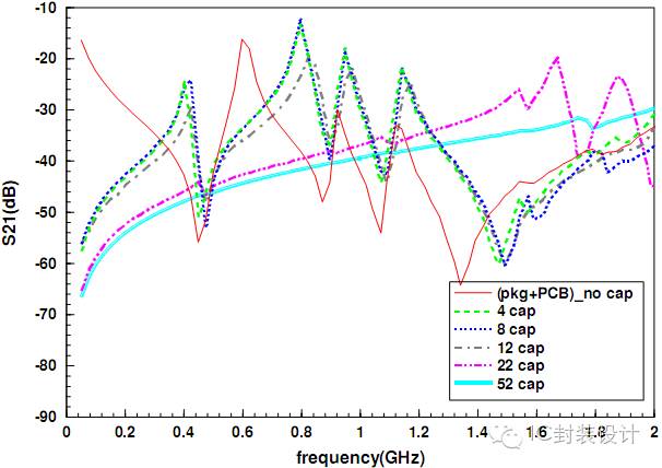 Figure 10: Effect of Number of Capacitors on |S21|
The results show that adding 4 or 8 capacitors effectively reduces |S21| between 0 and 200 MHz, but introduces a new resonance near 400 MHz. Adding 12 to 52 capacitors further suppresses low-frequency |S21|, reduces the 400 MHz resonance, and shifts the high-frequency resonance to higher frequencies with reduced amplitude. As the number of capacitors increases, noise suppression improves, especially between 300 MHz and 1.2 GHz (with 52 capacitors). Thus, increasing the number of capacitors enhances the power supply’s noise suppression capability.
Effect of Capacitance Value
On the Pkg+PCB structure, we placed capacitors with different values and observed the results in Figure 11. Comparing 100 nF and 100 pF, the 100 nF capacitor provides better suppression between 0 and 300 MHz, while the 100 pF capacitor performs better between 500 and 800 MHz. Using both 100 nF and 100 pF together results in worse performance than using them separately, with no clear advantage in low or high frequencies. Using 100 nF + 1 nF + 100 pF creates more resonance points, and if the noise aligns with these frequencies, it could amplify the noise, affecting or radiating the signal.
Therefore, the choice of capacitance value should depend on the frequency band to be suppressed. After determining the frequency band, the capacitor should be selected based on its resonance point. Lower capacitance values generally have better ESL and ESR characteristics.
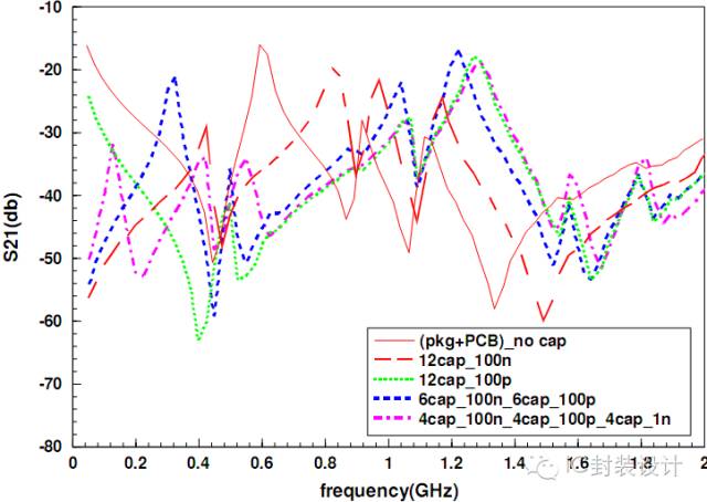
Figure 11: Simulation Results of Mixed Capacitance Values
Effect of Slab Thickness
First, we fixed the distance between the PCB power and ground planes at 0.7 mm and varied the Pkg power layer thickness to 1.6 mm, 0.8 mm, 0.4 mm, and 0.15 mm. The results are shown in Figure 12. As the Pkg power layer thickness increases, the first zero point shifts to lower frequencies. According to previous conclusions, noise below 2 GHz comes from the PCB. The results show that PCB-coupled noise increases, and after 2 GHz, the package becomes the main factor. |S21| increases with thickness, showing that the Pkg power plane thickness significantly affects the S parameter.

Figure 12: Effect of Pkg Power Layer Thickness on |S21|
Next, we kept the Pkg thickness at 0.15 mm and changed the PCB thickness to 0.15 mm, 0.4 mm, 0.8 mm, and 1.6 mm. The effect of PCB thickness on the S parameter is shown in Figure 13. The trend of PCB power layer thickness has little effect overall, with minor differences in the low-frequency region. As thickness increases, the first zero point shifts slightly, and the high-frequency part shows slight variations.
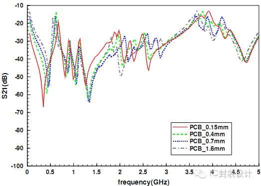 Figure 13: Effect of PCB Power Layer Thickness on |S21|
Effect of Capacitor Placement Distance
We know that the decoupling capacitor should be placed as close as possible to the noise source to minimize inductance, allowing the capacitor to absorb glitches faster, reduce noise, and stabilize voltage. Reducing the power plane thickness also helps reduce parasitic inductance. In the simulation, we changed the distance between the capacitor and the test point to 1.7 cm and 0.2 cm, respectively. The Pkg and PCB power layer thickness was divided into two cases: one with Pkg at 0.15 mm and PCB at 0.7 mm, and another with Pkg at 1.6 mm and PCB at 0.7 mm. The capacitor used was 100 nF, with ESR of 0.04 Ω and ESL of 0.63 nH.
 Figure 14: Distance Between Capacitor and Test Point
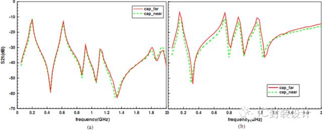 Figure 15: |S21| Simulation Results for Different Capacitor Distances
From the simulation results, if the capacitor cannot be placed near the noise source due to packaging constraints, reducing the Pkg power layer thickness can help minimize noise impact.
4. Conclusion
In conclusion, suppressing noise in high-speed digital circuits involves several key factors. The ideal position for decoupling capacitors is on the Pkg. While increasing ESR can flatten the pole, it also deepens the resonance frequency, increasing charging and discharging time, thus reducing the effectiveness of lowering power plane impedance. Increasing ESL leads to a faster rise in impedance after the resonance point, so lower ESL is better. More capacitors generally mean better noise suppression, improving isolation. Choosing the right capacitance value depends on the noise frequency band. Mixing values can broaden the noise suppression range but may increase resonance points, potentially amplifying noise if it falls on those frequencies. The PCB power plane thickness has minimal effect on Pkg, but the Pkg thickness influences PCB-coupled noise. Thinner Pkg layers reduce coupled noise, and at high frequencies, thinner layers lead to lower |S21| values.
Portable battery storage system,emergency power supply,portable solar power,off-grid solar system,household moveable solar energy
EMoreShare International Trade (Suzhou) Co., Ltd , https://www.emoreshare.com