
Low temperature co-fired ceramic (LTCC) technology is an advanced multi-layer substrate process that emerged in the mid-1980s. This innovative technology uses a unique material system, allowing it to be sintered at a relatively low temperature, which makes it compatible with metal conductors. The co-firing process significantly enhances the performance of electronic devices by improving their electrical and mechanical properties.
This paper presents a design for a miniaturized, low-noise amplifier (LNA) tailored for wireless local area networks (WLANs), leveraging the benefits of LTCC technology. Low-noise microwave amplifiers (LNAs) are widely used in various applications such as microwave communications, GPS receivers, remote sensing, radar systems, electronic warfare, radio astronomy, geodetic mapping, and high-precision measurement systems. As industrial technologies continue to evolve, the demand for miniaturization has increased, making LNAs more compact and efficient.
1. Technical Advantages of LTCC
Compared to conventional FR4 substrates, LTCC offers significant advantages at high frequencies. Its three-dimensional multi-layer integration capability allows for a much smaller form factor compared to traditional microwave substrates like Teflon PTFE. Additionally, LTCC materials have a wide range of dielectric constants, making them adaptable to different frequency bands. Compared to HTCC, the low sintering temperature of LTCC enables the use of low-melting-point, low-loss conductor pastes such as silver and gold, reducing signal loss. Furthermore, its thermal expansion coefficient closely matches that of semiconductor processes, facilitating better active and passive integration.
LTCC materials exhibit excellent high-frequency and high-Q characteristics, supporting operation up to several tens of GHz, which meets the demands of advanced RF and microwave applications.
- High Conductivity: Silver, gold, copper, and their alloys are used as conductor materials, improving the quality factor of the circuit and minimizing conductor losses.
- High Integration: LTCC can support dozens or even hundreds of layers, enabling the embedding of multiple passive components such as resistors, capacitors, inductors, EMI suppression elements, and more. It also supports surface mounting of active devices, enhancing integration density.
- Thermal Performance: LTCC provides better thermal conductivity than standard PCB substrates, making it suitable for high current and high-temperature environments.
- Reliability: LTCC is highly reliable, capable of withstanding high temperatures, humidity, and vibration, making it ideal for harsh environments such as military communications, aerospace, and automotive electronics.
- Cost-Effective: The discontinuous production process allows for inspection of raw ceramic substrates, increasing yield and reducing manufacturing costs.
2. Overall Design
2.1 Low Noise Amplifier Design Principle
A low-noise amplifier (LNA) differs from a general-purpose amplifier in that it prioritizes noise matching over maximum gain. This results in a slightly lower gain, known as the "correlation gain," which is typically 2–4 dB less than the maximum gain.
2.2 Performance Specifications, Device Selection, and Single Stage Circuit Simulation
The design employs a two-stage amplification configuration. The key specifications include a noise figure of ≤0.8 dB, a gain of ≥24 dB, a gain flatness of ±0.5 dB, and input/output VSWR ≤1.3 across the DC–14 GHz band.
For the first stage, the ATF55143 transistor was selected due to its high gain, low noise figure, small size, low power consumption, stable bias point, and reduced self-excitation. The board uses Ferro’s A6 diaphragm, incorporating built-in inductance and capacitance for enhanced mechanical strength. The board thickness is 0.6 mm.
Figure 1 shows the schematic of the first stage biasing and matching circuit. The proper selection of components such as C1, L1, C2, and L2 plays a critical role in achieving desired noise performance, S11, S22, and gain levels. These L/C high-pass filter circuits help suppress low-frequency oscillations, while R1 and R2 reduce leakage current and stabilize low-frequency signals.
C3 and C6 serve as bypass capacitors for filtering and stabilization, while R3 and R4 provide appropriate gate bias voltage. Source-level series negative feedback ensures overall stability, with microstrip lines acting as small inductors, offering simplicity, cost savings, and ease of debugging.
The second stage utilizes the RFMD SPF-5043Z monolithic amplifier, which offers a compact size, low noise, simple power supply requirements, and good stability. Both stages are powered from a single supply, with low voltage and current for easy adjustment.
2.3 Debugging and Optimization of Two-Stage Circuit
During the integration and debugging of the two-stage circuit, challenges mainly arose from stability issues and the possibility of the input VSWR not meeting standards. After simulation, many parameters did not match real-world conditions, such as capacitor and inductor values being inaccurate or line widths too narrow. Simply connecting single-stage circuits without optimization often led to failures in meeting the design specifications.
Figure 2 illustrates the simulation results of the entire circuit. These findings emphasize the importance of careful tuning and optimization to achieve the required performance metrics.
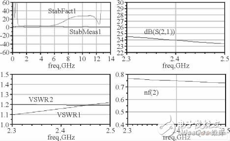
Figure 2: Overall Circuit Simulation Results
heat shrinkable cap
heat shrinkable cap,Heat-shrink tube,Heat shrinkable tubing,thermal contraction pipe,Shrink tube
Mianyang Dongyao New Material Co. , https://www.mydyxc.com