
**RF Card Design Principles and Implementation**
Non-contact IC cards, also known as RF cards, are a cutting-edge technology that has emerged in recent years. They combine RFID (Radio-Frequency Identification) and IC card technologies to solve the problem of passive operation (no internal power source) and eliminate the need for physical contact. The internal structure of a MIFARE 1 RF card includes several functional modules, as illustrated in Figure 1 below.
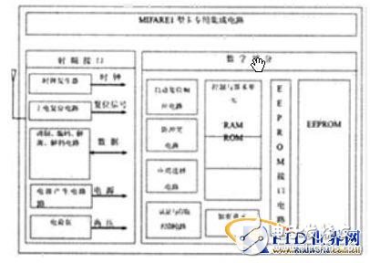
The MIFARE 1 RF card contains 1024 × 8-bit EEPROM memory, divided into 16 sectors with 4 blocks each. The RF interface module performs multiple key functions, including power generation, data communication, and secure authentication. Since the card itself does not have an internal power source, it relies on a power generation circuit to rectify, filter, and stabilize the voltage from the electromagnetic field generated by the reader. This process provides the necessary power for the card’s internal operations.
The digital part of the chip consists of various circuits, such as the reset response circuit, which automatically sends card information to the reader during power-on initialization, allowing the reader to identify and interact with the card correctly. The anti-collision circuit ensures that when multiple cards are present, only one is selected at a time, while others are put into a suspended state. The application selection circuit enables the card to support multiple applications, and the authentication and access control circuit verifies passwords and access rights. The control and arithmetic unit manages configuration, data processing, and encryption, while the encryption unit secures data transmission. The EEPROM interface handles read/write operations, and the EEPROM itself stores the data.
The MIFARE 1 RF card has a capacity of 8K bits, with a data retention period of up to 10 years. It can be rewritten up to 100,000 times and read unlimitedly. It operates without an internal power source and uses its own antenna. The card contains encryption logic and communication circuits, and communication between the card and the reader uses the international DES and RES secret cross algorithm, ensuring high security.
The working principle of the MIFARE 1 RF card involves an antenna and an ASIC (Application-Specific Integrated Circuit). The antenna consists of a few winding coils, making it ideal for integration into standard ISO cards. The ASIC features a high-speed interface (106 kbps) and includes a control unit and an 8K-bit EEPROM.
When the reader emits electromagnetic waves at a fixed frequency (13.56 MHz), the card's LC series resonant circuit matches this frequency, generating resonance. This causes a charge to build up in the capacitor, which is then transferred through a single-pass electronic pump to another capacitor for storage. Once the voltage reaches approximately 2V, it is used as a power supply for the card's circuits, enabling data transmission or access.
The design of the RF card's power generation circuit is crucial. It consists of two main parts: the RF interface circuit and the digital circuit. The RF interface handles energy coupling and signal transmission, which are key advantages of RF cards. The RF signal from the reader is converted into DC power through coupling, rectification, filtering, and voltage regulation.
**Coil Coupling**
L1 and L2 represent the primary and secondary coils of the antenna. L2 receives high-frequency electromagnetic waves from L1 at 13.56 MHz, producing a voltage across its terminals. At this frequency, L2 forms a series resonant circuit with equivalent inductance, capacitance, and resistance. The induced voltage depends on the energy of the emitted wave and the distance between the card and the reader.
**Rectification and Filtering**
The voltage from the antenna is sent to a full-wave rectifier (FWR) via a coupling capacitor C, converting it into a unidirectional AC signal. A filter capacitor CP removes high-frequency components, providing a DC voltage for the card. This capacitor also acts as an energy storage device to support the load.
**Voltage Regulation**
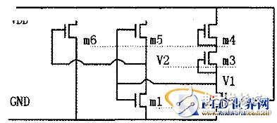
The output voltage from the filter capacitor is unstable and varies with the distance between the card and the reader. A voltage regulator circuit stabilizes it around 3.5V using series-connected saturated MOS transistors. The Rload represents the total internal resistance of the card’s circuits. Under normal conditions, the power generation circuit provides about 3.5V DC at Rload = 910Ω.
A detailed diagram of the voltage regulator circuit is shown in Figure 2 below.
This comprehensive design ensures reliable operation of the RF card, even in varying environmental conditions.
Surface Mount Assembly,print circuit board assembly,Smt Assembly Pcba,smt pcba board
Dongguan Jinglin Communication Technology Co., Ltd. , https://www.jlpcba.com