Introduction to RF card design principles and implementation

RF Card Design Principles and Implementation 
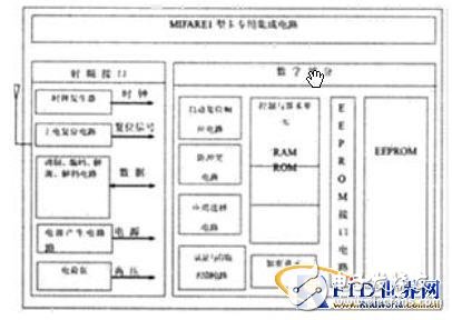
Non-contact IC cards, also known as RF cards, are a recent technological advancement that combines RFID technology with traditional IC card systems. This innovation successfully addresses the challenge of passive operation (no internal power source) and eliminates the need for physical contact. The internal structure and working principles of the MIFARE 1 RF card are illustrated in Figure 1 below.

Design of power supply in antenna card in RF card

The MIFARE 1 RF card contains 1024 × 8-bit EEPROM memory, organized into 16 sectors, with 4 blocks per sector. The RF interface module performs several key functions, including communication, data storage, and security management. Since the card has no internal power source, it relies on a power generation circuit to rectify, filter, and stabilize the voltage from the electromagnetic field generated by the reader. Each block in the digital part of the chip serves a specific purpose. The reset response circuit automatically sends card information to the reader during a power-on reset, allowing the reader to identify the card type and respond accordingly. The anti-collision circuit ensures that only one card is active at a time when multiple cards are in the reader's range. The application selection circuit allows the card to function as "multi-purpose," enabling users to choose different applications stored within the card. The authentication and access control circuit verifies passwords and access rights, ensuring secure data access. The control and arithmetic unit manages configuration, data processing, and operations like addition and subtraction. The encryption unit secures communication between the card and the reader, while the EEPROM interface handles reading, writing, and decoding of data stored in the memory. RF Card Design Principles The MIFARE 1 (M1) RF card has an 8K-bit capacity, with a data retention period of up to 10 years. It can be rewritten over 100,000 times and read unlimited times. Unlike traditional smart cards, the M1 card does not have an internal battery but instead uses an embedded antenna. It includes encryption logic and communication circuits, and communication between the card and reader uses international DES and RES secret cross algorithms, offering high security. Working Principle The M1 RF card consists of an antenna and an ASIC (Application-Specific Integrated Circuit), with no external components. The antenna is made up of a few sets of winding coils, making it suitable for packaging into ISO standard cards. The ASIC features a high-speed (106 kbps) interface, including a control unit and an 8K-bit EEPROM. When the reader emits a fixed-frequency electromagnetic wave, the card's LC series resonant circuit matches the frequency, generating resonance. This resonance charges a capacitor, which then powers the card’s circuits through a single-pass electronic pump. Once the charge reaches approximately 2V, it serves as a power source for data transmission or access. Design and Application of the RF Card Power Generation Circuit An RF card comprises two main parts: the radio frequency interface circuit and the digital circuit. One of its key advantages is the ability to generate power wirelessly and transmit signals without a direct connection. This is achieved through coupling, rectification, filtering, and voltage regulation within the card. Coil Coupling L1 and L2 represent the primary and secondary coils of the antenna. L2 receives high-frequency electromagnetic waves from L1 (at 13.56 MHz), producing a voltage across its terminals. At this frequency, L2 forms a series resonant circuit with equivalent inductance, capacitance, and resistance. The induced voltage depends on the energy emitted by the reader and the distance between the card and the reader. Rectification and Filtering The voltage obtained from the antenna is sent to a full-wave rectifier (FWR) through a coupling capacitor (C), converting it into a DC signal. A filtering capacitor (CP) smooths out the high-frequency signal, providing a stable DC power supply. The capacitor also acts as an energy storage device to support the load. Regulator Circuit The output voltage from the filter capacitor (VDD) is unstable and varies depending on the distance between the card and the reader. A voltage regulator circuit stabilizes this voltage to around 3.5V. This is achieved using several series-connected saturated MOS transistors. Rload represents the total internal resistance of all circuits in the card. Under normal operating conditions, the power generation circuit can provide about 3.5V DC to the card’s circuits after passing through Rload = 910Ω. A detailed diagram of the voltage regulator circuit is shown in Figure 2.

Design of power supply in antenna card in RF card

PCB Layout Service

Pcb Assembly Line,Pcb Prototype Assembly,Pcb Layout Design Services,order custom pcb

Dongguan Jinglin Communication Technology Co., Ltd. , https://www.jlpcba.com