
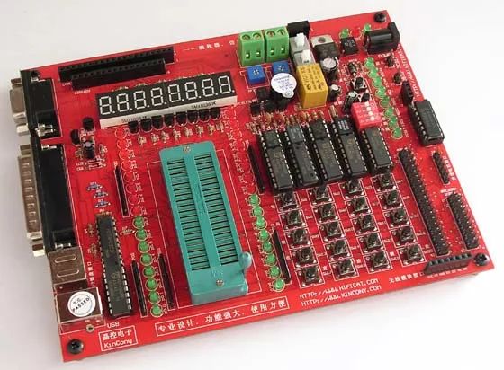
Figure 1: Picture of the host part of the 51 MCU integrated learning system

Figure 2: Supporting tutorial for the 51 MCU comprehensive learning system - "MCU Quick Start"
The images above show the hardware platform of the 51 MCU integrated learning system that we will use. As seen in Figure 1, this experiment uses the integrated system host along with the onboard ADC0832 analog-to-digital conversion chip. You can explore the principles and usage of other functional modules within the integrated system through previous issues of the "Electronic Production" magazine and post-production tutorials. In industrial control and smart instrumentation, real-time control and real-time data processing are typically handled by microcomputers. However, the information processed by computers is always digital, while the parameters being controlled or measured often involve continuously varying analog quantities, such as temperature, speed, pressure, etc. These are usually represented as analog electrical signals. Analog storage and processing are difficult, not suitable for long-distance transmission, and prone to interference. In most industrial application systems, sensors convert non-electrical analog signals into corresponding analog signals, which are then converted into digital signals for processing via an analog-to-digital (ADC) circuit. This forms a complete signal chain, and the analog-to-digital conversion process is what we commonly refer to as the ADC circuit. **Introduction to Analog-to-Digital Conversion (ADC)** **ADC Conversion Principle** The conversion principle of ADC varies depending on the type of ADC circuit used. Typically, an ADC circuit consists of two parts: a sample-and-hold circuit and a quantization and coding circuit. Among these, the quantization and coding circuit is the core component, and all ADC circuits must include it. There are several types of ADC circuits, which can generally be categorized into two groups: - **Indirect Method**: Converts the sampled and held analog signal into a time or frequency proportional to the analog quantity, then converts it into a digital value. This is usually done using a clock counter, also known as a counter. Its working characteristics include low speed, high precision, and strong anti-interference capability. - **Direct Method**: Converts the signal into a digital value by comparing the reference voltage with the sample-and-hold signal. It has high speed and is easy to achieve accurate conversion. The analog-to-digital conversion process involves four stages: sampling, holding, quantizing, and encoding. Sampling is the process of converting a continuous-time signal into a discrete-time signal. After sampling, the original continuous-time and continuous-value analog signal becomes a discrete-time and continuous-value signal known as a sampled signal. The sampling circuit acts like an analog switch that operates periodically. In theory, the switch closes for a very short period during each cycle, and at the moment the switch closes (sampling time), we take a "sample" of the analog signal. Quantization is the process of converting a continuous numerical signal into a discrete numerical signal. After quantization, the time-discrete and numerically continuous sampled signal becomes a time-discrete and numerically discrete digital signal. Since digital quantities in circuits are typically represented in binary code, there is an encoding circuit following the quantization circuit that converts the value of the digital signal into binary code. However, quantization and encoding take some time, so a hold circuit is placed before the quantization circuit. The hold process converts a time-discrete and numerically continuous signal into a time-continuous and numerically discrete signal. During quantization and encoding, the hold circuit acts as a constant voltage source that "holds" the signal voltage at the sampling instant at the input of the quantizer. Although the logical keeper is a separate unit, in engineering practice, the holder is always combined with the sampler. Together, they are referred to as a sample-and-hold unit. **Introduction to the 8-bit Serial A/D Converter ADC0832** The ADC0832 is an 8-bit resolution, dual-channel A/D converter from National Semiconductor. Due to its compact size, strong compatibility, and cost-effectiveness, it is widely popular among MCU enthusiasts and enterprises, making it highly adopted in the market. The ADC083X series is a family of serial analog-to-digital converters commonly found on the market. Examples include ADC0831, ADC0832, ADC0834, and ADC0838. These are 8-bit serial I/O analog-to-digital converters with multiplexer switches, featuring fast conversion speeds (conversion time of 32μS), single power supply, and low power consumption (15mW), making them suitable for various portable smart meters. This chapter uses the ADC0832 as an example to demonstrate its usage. The ADC0832 is an 8-pin dual-in-line, dual-channel A/D converter capable of performing analog-to-digital conversion on two analog signals. It can operate in both single-ended input mode and differential mode. The ADC0832 uses serial communication for channel selection, data acquisition, and data transfer via the DI data input. With 8-bit resolution (up to 256 levels), it meets general analog conversion requirements. The internal power supply input and reference voltage are multiplexed, allowing the analog voltage input of the chip to range between 0 and 5V. It features dual data output for data verification, reducing errors, and offers fast conversion speed and strong stability. Independent chip enable inputs make multi-device mounting and processor control more convenient. **Key Features of ADC0832:** - 8-bit resolution - Dual-channel A/D conversion - Input and output levels compatible with TTL/CMOS - Input voltage ranges from 0 to 5V when powered by 5V - Operating frequency of 250kHz, conversion time of 32μS - Low power consumption of only 15mW - Available in 8P, 14P-DIP, and PICC packages - Commercial grade operating temperature: 0°C to +70°C - Industrial grade operating temperature: -40°C to +85°C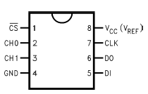
Figure 3: ADC0832 pin diagram
**Chip Interface Description:** - **CS_**: Chip Select Enable, active low. - **CH0**: Analog input channel 0, or used as IN+/–. - **CH1**: Analog input channel 1, or used as IN+/–. - **GND**: Chip reference ground. - **DI**: Data signal input, channel selection control. - **DO**: Data signal output, conversion result output. - **CLK**: Chip clock input. - **Vcc/REF**: Power supply and reference voltage input (multiplexed). **How the ADC0832 Works:** Under normal conditions, the interface between the ADC0832 and the microcontroller requires 4 data lines: CS, CLK, DO, and DI. However, since DO and DI are not used simultaneously during communication and the interface is bidirectional, they can be shared on one data line when I/O port resources are limited. When the ADC0832 is not operating, the CS input should be high, disabling the chip, and the CLK and DO/DI levels can be arbitrary. When performing an A/D conversion, the CS must be pulled low and kept low until the conversion is complete. At this point, the chip starts the conversion process, and the microcontroller sends clock pulses to the CLK input. The DO/DI terminal uses the data signal selected by the DI terminal for channel function. Before the falling edge of the first clock pulse, the DI terminal must be high to indicate the start signal. Before the second and third clock pulses fall, the DI terminal should input two bits of data to select the channel function. | Channel Address | SGL/DIF | ODD/SIGN | Working Mode Description | |------------------|---------|----------|---------------------------| | 0 | 0 | + | - | Differential mode | | 0 | 1 | - | + | Differential mode | | 1 | 0 | + | | Single-ended input mode | | 1 | 1 | | + | Single-ended input mode | After the third pulse falls, the DI terminal no longer affects the input, and the DO/DI terminal begins to output the converted data. From the fourth pulse’s falling edge, bit 7 of the conversion data is output via the DO terminal, followed by the next bit on each subsequent pulse. The lowest bit, Data0, is output after the 11th pulse, completing the byte of data. The next byte starts from the 11th pulse, with Data0 being output from the falling edge of the 11th pulse. The 8-bit data is then output, and the data output is completed by the 19th pulse, marking the end of the A/D conversion. Afterward, the CS is set high to disable the chip, and the converted data can be directly processed. Refer to Figure 4 for timing details. When used as a single-channel analog input, the ADC0832 accepts an input voltage ranging from 0 to 5V, with an 8-bit resolution providing a voltage accuracy of approximately 19.53mV (5/256 V). If used with IN+ and IN- inputs, the voltage range can be expanded, increasing the conversion range. However, it is important to note that if the voltage at IN- is higher than that at IN+, the resulting converted data will always be 00H. **ADC0832 Operating Timing**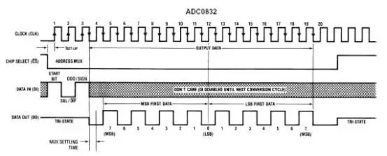
Figure 4: ADC0832 working sequence
**ADC0832 Software and Hardware Design Example** After studying the theory outlined above, you should now have a good understanding of analog-to-digital conversion. To deepen your practical knowledge, we will apply the ADC0832 in a real-world scenario. The purpose of this example is to display the voltage sampled on channel 1 on an LED digital tube and observe how the output changes as the input voltage on channel 1 is adjusted. Before debugging this example, make sure the function selection switch is set to the position for ADC0832, as shown in Figures 5 and 6.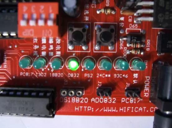
Figure 5: ADC0832 experimental demonstration
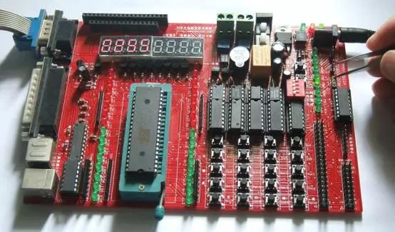
Figure 6: ADC0832 experimental demonstration
**Hardware Schematic**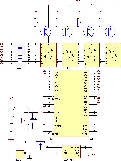
Figure 7: Hardware schematic
**Program Flow Chart**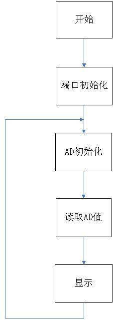
Figure 8: Software flow chart
A Wi-Fi 5 ONU is a versatile device that plays a crucial role in delivering high-speed internet over fiber optic networks while providing robust wireless connectivity. When selecting a Wi-Fi 5 ONU, consider factors such as speed, coverage, number of Ethernet ports, and additional features that suit your specific networking needs.
Wi-Fi 5, also known as 802.11ac, is a wireless networking standard that provides high-speed Wi-Fi connectivity, primarily in the 5 GHz band. When referring to Wi-Fi 5 ONUs, you are generally looking at devices that serve as the interface between a passive optical network and the end users, while also providing wireless connectivity. Here are some different types of Wi-Fi 5 ONUs, categorized based on their features and capabilities:
Dual-Band WiFi 5 ONU: It supports both 2.4 GHz and 5 GHz bands, allowing for greater flexibility in device connectivity.
Multi-Service WiFi 5 ONU: It combines ONT functionality with support for multiple services, such as VoIP and IPTV, in addition to Wi-Fi. That is WiFi 5 ONT with CATV, WiFi 5 ONT with VOIP.
Integrated Router WiFi 5 ONU: It combines ONU functionality with a built-in router, providing both wired and wireless connectivity from a single device.
Wi-Fi 5 Mesh ONU: It incorporates mesh networking capabilities, allowing multiple devices to work together to provide seamless Wi-Fi coverage throughout larger areas.
dual band wifi xpon onu,5g gpon ont,ftth gpon onu,catv wifi5 xpon onu,catv gepon onu
Shenzhen Runtop Technology Co.LTD , https://www.runtoptech.com