
| TD-SCDMA RD V2.1 design that meets Rx blocking mask and sensitivity requirements |
| Abstract: This application note introduces Maxim ’s second-generation TD-SCDMA RF transceiver chipset and its V2.1 reference design. It also discusses some key system issues, such as sensitivity and blocking signal testing, to help you establish the best TD-SCDMA RF design after careful consideration. Maxim's TD-SCDMA RF transceiver chipset Maxim's TD-SCDMA mobile phone RF chipset consists of MAX2507 (Tx) and MAX2392 (Rx). Both RF ICs are manufactured using Maxim's indoor high-frequency process technology. The MAX2507 is a fully integrated transmitter chip that includes circuits from analog I / Q input to power amplifier output. Its main functional modules are I / Q quadrature modulator, upconverter, adjustable gain amplifier (VGA), RF voltage controlled oscillator (VCO) and phase-locked loop (PLL), IF local oscillator and RF power amplifier ( PA). The device is packaged in a 7mm x 7mm surface grid array (LGA). The MAX2392 is the corresponding zero-IF receiver, including the circuit from the low-noise amplifier (LNA) to the analog I / Q output. Its main functional modules are LNA, RF I / Q demodulator, RF VCO and PLL circuit, baseband channel selection filter, DC offset calibration circuit, and automatic gain control (AGC) baseband amplifier. The MAX2392 is available in a 5mm x 5mm QFN package. The complete reference design using the OEM RF RF board shows that the actual total PCB area is 6.6cm². The functional structure of the reference design is shown in Figure 1, and Figure 2 is a photo of the reference board. The requirements of TD-SCDMA standard for Rx The main requirements of TD-SCDMA standard for Rx are shown in Table 1. The minimum sensitivity that must be met is -108dBm, and the blocking specification requires a valley shape with frequency offset. 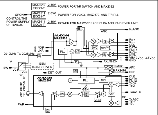 Figure 1. Functional structure diagram of TD-SCDMA reference design 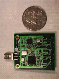 Figure 2. TD-SCDMA reference design board Table 1. TD-SCDMA Rx requirements
Sensitivity and blocking requirements Analysis and measurement results Receiver sensitivity is a system specification index, which is greatly affected by the RF channel signal quality and DSP modem baseband processing capabilities. At the minimum input signal level, the RF channel quality is mainly limited by the receiver's noise contribution, which is determined by the noise figure (NF). Note that under these signal conditions, the receiver phase noise is not considered because its level is much smaller than the thermal noise. Therefore, receiver phase noise has minimal effect on input SNR degradation. In the 3GPP TR 25.945 standard [3], the receiver sensitivity is specified as -108dBm. According to typical baseband processing gain and modulated BER, the receiver sensitivity corresponds to 9dB maximum receiver NF. As shown in Figure 1, the measured NF of the receiver channel of the TD-SCDMA reference design is approximately 5.7dB. Therefore, the corresponding measured sensitivity is -111dBm, which has a margin of 3dB compared to the standard specification. The impact of in-band blocking signals on receiver performance is mainly manifested in three phenomena: cross-modulation, second-order intermodulation products, and intermixing, which are discussed in three sections below. Cross modulation 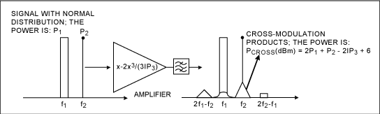 Figure 3. Cross-modulation products Figure 3 shows the cross-modulation phenomenon, which appears in nonlinear components such as amplifiers and mixers. In the figure, the f1 signal is a modulation blocking signal with a certain bandwidth, and the CW signal of f2 is the desired signal. At the output of the amplifier, a triangular intermodulation product centered at f2 appears near the desired signal spectrum. This cross-modulation product is usually related to the third-order nonlinearity of the device, which is the third-order cutoff point. When the blocking signal has a Gaussian white noise normal distribution characteristic, the power of the cross-modulation product can be estimated according to the following formula:  In the case where the input signal is also a modulated signal, the waveform of the output product is the convolution of the triangular wave and the signal power spectral density function. Since the characteristics of the blocking signal deviate from the Gaussian noise normal distribution, the cross-modulation products will be reduced. When the interference signal is a modulated envelope constant blocking signal, the cross-modulation product is zero. The 3GPP TDD standard stipulates that when the offset is ± 4.8MHz, the sensitivity degradation of 3dB allows -49dBm modulated interference signals. If we think that the result of sensitivity degradation only comes from the cross-modulation product, as long as the power of the cross-modulation product is relatively smaller than the receiver's in-band thermal noise power at the sensitivity level, this performance index can be achieved. Assuming that the noise figure of the receiver is less than 9dB specified in the standard, the third-order cut-off point of the receiver generated by cross modulation can be derived from Equation 2. Second order intermodulation products (IM2) 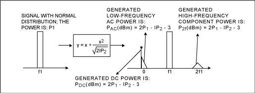 Figure 4. Second-order intermodulation products The second-order intermodulation products generated by the modulation blocking signal include three parts, as shown in Figure 4: DC offset, low-frequency products around 0 Hz, and products around 2f1. When the statistical characteristics of the blocking signal conform to the Gaussian noise normal distribution, the three parts are equal in power and can be estimated using the formula in Figure 4. When the statistical characteristics of the blocking signal are close to a signal with a constant envelope, the power of the low-frequency products will be minimized. When the interference signal is a blocking signal with a constant envelope, there is no low-frequency IM2 product at the output. At the I / Q output of the zero-IF receiver, these low-frequency and DC IM2 components fall within the required bandwidth of the down-converted signal, resulting in receiver performance degradation. In the MAX2392 receiver circuit, the on-chip DC offset is eliminated, so when calculating the receiver interference budget, only low-frequency IM2 products need to be considered. The 3GPP TDD standard stipulates that when the offset is ± 4.8MHz, the sensitivity degradation of 3dB allows a modulated interference signal of -49dBm. Similar to the case of cross-modulation, if we think that the sensitivity degradation results only from low-frequency IM2 products, and the NF of the receiver is less than 9dB specified in the standard, the required receiver second-order cutoff points IIP2, RX can be estimated, as shown in Equation 3. Assuming that the down-conversion in-band blocking signal is eliminated in the post-mixing baseband channel selection filter, the receiver second-order cutoff point is only determined by the zero-IF down-converter blocking signal.  Note: "-3" is related to the modulation factor. MAX2392 has four working modes. When there is a large blocking signal, it is recommended to use high gain high linearity (HGHL) and high gain medium linearity (HGML) modes for receiving weak signals. For the receiver of the reference design, both modes will measure IIP2, RX ≥ + 15dBm, which meets the requirements and has a margin of at least 12dB. Phase noise and mutual mixing The 3GPP TD-SCDMA standard does not clearly specify the phase noise of the VCO; it is taken from other relevant specifications. As mentioned earlier, the transmitter EVM is one of the parameters affected by the transmitter VCO + PLL phase noise, it does not have strict requirements on the phase noise of RF equipment. Receiver sensitivity is also related to LO phase noise, but even in the case of 16QAM modulation, there is no strict phase noise requirement for RF equipment. The two specifications that have strict requirements for LO phase noise are the minimum requirements for blocking and dual-frequency intermodulation. These specifications have requirements for intermixing of interfering signals or LO sideband noise modulation, as shown in Figure 5. 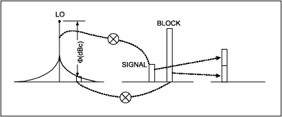 Figure 5. Interference signal LO phase noise mixed with each other As discussed in the blocking and dual frequency intermodulation requirements, in these test cases, the receiver sensitivity is allowed to degrade by 3dB. We assume that all the degradation comes from the phase noise mixing with each other, and the receiver noise figure is less than the 9dB specified in the specification. We can use the following formula to calculate the required LO phase noise:  The maximum interference power in the blocking and dual-frequency intermodulation test is -46dBm when it is offset from the signal center frequency by ± 3.2MHz. Taking this value into the above formula, when the carrier is offset by 3.2MHz, the receiver LO phase noise is less than -119dBc / Hz. The phase noise measured by the MAX2392 VCO is -129dBc / Hz, which meets the requirements and has a 10dB margin. For four-way out-of-band blocking, the SAW filter before the LNA suppresses all out-of-band interference and reduces its level to avoid LNA compression. Since the level of the blocking signal at the output of the LNA is very low compared to the mixers IP2 and IP3, there is no need to use a SAW filter between the LNA and the mixer. The interstage filter provides the required balun function, so more filtering functions can be obtained without increasing the cost. For example, when the offset is ± 85MHz, the specified blocking signal is -15dBm. If the SAW provides 30dB attenuation, the LNA's blocking signal level is -46dBm (T / R switch has 1dB loss), close to the in-band blocking signal level, and the above method can be used to analyze IM2 and IM3. The measurement results show that when testing each blocking signal, 3GPP requires a margin of at least 3dB. Conclusion Maxim's TD-SCDMA reference design V2.1 fully complies with the requirements of the 3GPP standard, and has at least a 3dB margin on all key receiver specifications. | |||||||||||||||||||||||||||||||||||||||||||||||||||||||||||||||||||||||||
There are plenty of benefits for using usb type c cable For starters, the port is reversible! But that is only the tip of the cable. And like ice bergs, there is much more than meets the eye in type c cables. They allow for faster transfers, charging, 4K monitor output and more.
Needless to say we will have to start populating our living spaces with USB 3.1 Type C and accessories.It measures in at 1.8 meters of length and can handle USB 2.0 charging, as well as up to 60W of fast charging power. Not bad at all.
USB Type C Cable, USB 3.1 Type C, Type C Cable, USB Type C
Hebei Baisiwei Import&Export Trade Co., LTD. , https://www.baisiweicable.com