
At present, most of the long-term thermal trip test schemes adopted in China use a transformer to directly apply a voltage to the circuit breaker to obtain a test current. During the test, due to the fluctuation of the grid voltage, the change of the lead resistance in the current-carrying circuit, and the change in the resistance of the load itself, the test current changes accordingly, and it is difficult to meet the requirements of the national standard. This paper introduces a power regulated inverter power supply, which has the advantages of stable and reliable operation, high input power factor, high output precision, small waveform distortion and high efficiency.
Inverter power supplies with a nominal power of 300W are not a problem for home electric fans, televisions, and daily lighting. The 300W inverter uses 12V/60AH batteries to supply power to the above household appliances. After a full charge, it can be used for nearly 5 hours. However, even if the battery voltage is sufficient, it is still difficult to start the 180-liter refrigerator, and the output voltage drops to less than 180V at the start of the startup. The nominal power of the refrigerator compressor is about 100W. The actual starting current can reach more than 2A. If the starting voltage is not very obvious, the output power must be increased to 600VA. If the output power is increased, The PWM voltage regulator system can significantly reduce the step-down amplitude of the startup. Regardless of the electric fan or the refrigerator, when applying the inverter power supply, the LC filter in Figure 1 should be added at the output of the inverter to improve the waveform and avoid the pulse rising edge rushing through the motor winding.

figure 1
In an inverter using a bipolar switching transistor, the base driving current is substantially 1/β of the switching current. Therefore, the high current switching circuit must adopt multi-stage amplification, which not only complicates the circuit, but also degrades reliability and When the output power is increased, the switching tube driving current needs to be larger than 1/β of the collector current, so that the ordinary driving IC cannot be directly driven. Although multi-stage amplification can achieve the purpose, the waveform distortion is significantly increased, resulting in an increase in the on/off loss of the switching tube. At present, the driving schemes for high-power inverter power supplies and UPS are mostly solved by using MOS FET tubes as switching devices.
MOSFET application
In recent years, the manufacturing process of metal oxide insulated gate field effect transistors has been rapidly developed, making it difficult to achieve a drain-source voltage withstand voltage (VDS) of more than kV and a drain-source current (IDS) of 50A, which is widely used. High frequency power amplification and switching circuits.
In addition, there is a hybrid product of a bipolar transistor and a MOS FET tube, a so-called IGBT insulated gate bipolar transistor. As its name suggests, it is a combination of MOS FET tubes as a preamplifier and bipolar transistor as an output. Therefore, the IGBT has both the voltage driving characteristics of the insulated gate field effect transistor and the output characteristics of the bipolar transistor with low saturation voltage drop and high withstand voltage. The turn-off time is less than 0.4 μs, the VCEO is 1.8 kV, and the ICM reaches The level of 100A is currently used in circuits such as motor variable frequency speed regulation, high power inverters and switching power supplies.
Generally, a medium-power switching power supply inverter is commonly used in a parallel push-pull circuit of a MOS FET tube. MOS FET tube drain-source conduction resistance, with the current sharing characteristics of the resistor, parallel application does not need to add a current sharing resistor, the drain source directly parallel application. When the gate and source are used in parallel, each MOS FET must use a separate gate isolation resistor to avoid the increase of the total capacitance of the gate capacitance of each switch, resulting in an increase in the charging current and delaying the establishment of the driving voltage. The conduction loss of the switch tube increases.
MOSFET drive
In recent years, with the improvement of the MOSFET production process, various switching power supplies and converters have widely used MOS FET tubes as high-frequency high-voltage switching circuits. However, integrated circuits dedicated to driving MOS FET tubes are rare in China. The requirement for driving the MOSFET is a low output impedance with a sink current drive circuit. Therefore, a driver IC commonly used for a bipolar switch can not be directly used to drive a field effect transistor.
At present, there are still a small number of ICs that can directly drive MOSFETs. The UC3842 series is commonly used for single-ended drivers, and the SG3525A (drive N-channel FET) and SG3527A are used for push-pull circuits. Drive P-channel FET and SG3526N (drive N-channel FET). However, in the nearly 40 years of rapid development of switching power supplies, there have been a large number of excellent and fully functional double-ended output driver ICs. At the same time, with the popularization of MOSFET applications, many new circuits have been developed, which can be used for Driving the MOSFET tube to solve the MOSFET drive includes nothing else: one is to reduce the output impedance of the driver IC; the other is to add a sink current path of the MOSFET. To this end, it may be worthwhile to review the driver stages of the SG3525A, SG3527A, SG3526N, and the single-ended driver UC3842 series.
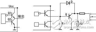
figure 2
Fig. 2a shows the driving output circuit of the above IC (taking one of the outputs as an example). The output pulse of the oscillator passes through the NOR gate, and the rising and falling edges of the pulse output two driving pulses with different timings. During the pulse forward period, Q1 is turned on, Q2 is turned off, and the positive pulse of the Q1 emitter output charges the gate capacitance of the switch, so that the drain-source quickly reaches the turn-on threshold. When the forward pulse is over, if the charge between the gate and the source of the switch cannot be quickly discharged, the drain-source drive pulse will not be cut off immediately. For this reason, after Q1 is turned off, the NOR gate immediately turns on Q2 to provide a path for the gate-source capacitor discharge. In this drive mode, Q1 provides the drive current and Q2 provides the sink current (ie, the discharge current). Q1 is the emitter output, which itself has a very low output impedance.
In order to meet the above requirements, the common peripheral driving circuit for the bipolar switching tube drive output is connected to the peripheral driving circuit of FIG. 2b, and the driving requirement of the MOS FET tube can also be satisfied. Designing an integrated circuit for driving a bipolar switch tube, the two-terminal totem pole output is often used to output two pulses, that is, the two output pulse polarities are the same to drive the two NPN transistors of the push-pull. In order to make the push-pull tubes turn on in turn, the timing of the two drive pulses is different. If the first channel outputs a positive pulse, after the cutoff, after a dead time, the second way starts to output. The two-drive stage uses a bipolar transistor collector open-circuit output to achieve different pulse polarities for driving NPN-type or PNP-type switches.
The emitter of the internal buffer of the pre-driver IC establishes a non-inverted positive polarity drive pulse on the load resistor R1 to turn off the transistor Q. At the rising edge of the drive pulse, the positive polarity pulse is applied to the gate-source of the MOS FET switch via diode D to charge the gate-source capacitor CGS. When the charge voltage reaches the gate voltage threshold of the switch, its drain-source is turned on. . After the positive pulse duration, the IC internal buffer amplifier emitter level is zero, and the output will have a dead time for a certain period of time. At this time, the emitter of Q has a CGS charging voltage, so Q is turned on, CGS is discharged through the ec pole of Q, and the collector current of Q is a sinking current path. R2 is the gate resistance of the switch tube. The purpose is to prevent the gate of the switch tube from floating during the Q and D conversion process. Otherwise, the approximately infinite high input impedance is easily broken down by the interference level. In this way, a common double-ended output integrated circuit is used to drive the MOS FET switch tube, which can achieve an ideal effect. In order to reduce the on/off loss, D should use a fast switching diode. The collector current of Q should be determined according to the switching transistor. If multiple output MOS FETs are used in parallel for each output in order to increase the output power, a perfusion transistor with a large ICM and a high-speed switching diode should be selected.
8" Novelty Candle have 22g 23g 25g sell very well for Jeddah market . 8" Novelty Spiral Candle can do your own brand and logo .boxes. each box have 12pcs, each carton have 24boxes. Novelty Scented Candles have many colors , such as white , yellow ,green ,blue ,red and so on . we are the biggest CANDLE FACTORY IN hebei province , We make sure the shipment is quick . usually about 30-35days after receiving the deposit and confirming the package .
Welcome to inquiry and welcome to order !
8" Novelty Candle
8" Novelty Candle,8" Novelty Spiral Candle,Novelty Scented Candles,Glass Jar Novelty Candles
Shijiazhuang Zhongya Candle Co,. Ltd. , https://www.zycandlefactory.com