
1 Introduction
LEDs were introduced in the early 1960s. Early LEDs had very low luminous efficiency (0.1 lm/W), low luminous flux (a few thousandths of lumens), and a single color (red), so they could only be used as indicators. Use, such as the power indicator on the tape recorder. With the development of semiconductor technology, the current L ED performance has been a breakthrough development, the luminous efficiency has reached tens of lumens per watt, the luminous flux reaches several lumens, the color is more diverse, there are red, orange, yellow, green Various colors such as blue and white have been greatly expanded in the field of application. In particular, the successful development of white LEDs has made it possible to use L ED in the field of lighting. In the past 100 years, lighting sources have undergone three important development stages. Incandescent lamps are the first generation of light sources, fluorescent lamps are the second generation of light sources, and high-intensity gas discharge lamps are the third generation of light sources. Now many people in the lighting industry are very optimistic about the prospects of LED, that this is the fourth generation of light source. This article will discuss some aspects of the application of L ED in the field of lighting, and look forward to its development prospects.
2 LED technology development
2.1 Materials
Light-emitting diodes (LEDs) were introduced in the 1960s. In 1964, the III-V luminescent material GaAsP was successfully developed, and red LEDs appeared, with a peak wavelength of about 650 nm. Although the driving current is 20 mA, the luminous flux of a single L ED is only a few thousandths of a lumen, and the corresponding luminous efficiency is only 0.1 lm / W, but the all-solid-state light source is beginning to be accepted, mainly used in the field of indicator lights.
In the 1970s, material research was more active and the first climax in the history of L ED development. The quality of GaAsP/GaAs has been improved, and the epitaxial materials have been fabricated by vapor phase epitaxy (VPE) and liquid epitaxy (LPE), which not only improves the light efficiency to 1 lm/W, but also covers the color from yellow-green to infrared. The spectral range (565 to 940 nm) has also begun to enter the display field.
After the 1980s, the application level gradually developed, packaging technology was gradually improved, and peripheral support conditions were relatively formed, which led to breakthroughs in L ED technology. For example, the GaAlAs epitaxial layer is fabricated by LPE technology to produce high-brightness red LEDs and infrared diodes (IL ED) with wavelengths of 660, 880, and 940 nm, respectively. With the development of metal organic chemical vapor phase epitaxy (MOVPE), a 780 nm semiconductor laser diode was produced; the red and yellow L ED light effect made with the new chip material Al InGaP can reach 10 lm/W, if transparent lining is used. At the bottom, the light efficiency can exceed 20 lm / W. In 1984, the third-generation semiconductor material GaN developed by MOVPE made the blue and green LEDs achieve a luminous efficacy of 10 lm/W, achieving full colorization of LEDs.
In the 1990s, technology development focused on white LEDs. There are roughly three ways to make white LEDs: a small amount of fluorescent material is applied to the surface of the blue chip, part of the blue light excites the coating material to form yellow light, and the blue light emitted by the transmitted chip itself constitutes white light; red, green and blue are used. The chips are packaged together; a single-chip white LED is fabricated by using ZnSe as a base. After being energized, the blue light emitted by the ZnSe active layer and the yellow light emitted from the center of the substrate are mixed into white light.
After entering the 21st century, L ED is known as the “new light source of the 21st century†and is the “fourth generation light source†after incandescent lamps, fluorescent lamps and high-intensity discharge lamps (HIDs). With the continuous development and innovation of materials technology and packaging technology, red and orange L ED light effects can reach 100lm / W, and green L ED can reach 50 lm / W. The luminous flux of a single LED also reaches tens of lumens. The high efficiency of LED, ultra-high brightness and full colorization have made its application field more and more popular, and gradually move toward outdoor lighting.
Usually, people use a light intensity of 1 cd as the demarcation point between a general L ED and a high-brightness LED. Currently, materials for making high-brightness LEDs are mainly AlGaAs, AlGa InP, and Ga InN. AlGaAs is suitable for high-brightness red and infrared LEDs, made of LPE; AlGa InP is suitable for high-brightness red, orange, yellow and yellow-green LEDs, made with MOVPE; Ga InN for high-brightness dark green, blue, violet and ultraviolet L ED, manufactured with high temperature MOVPE.
2.2 Chip structure
Taking the commonly used Al InGaP chip as an example, the substrate of Al InGaP L ED produced by Hewlett Packard is a 200 μm thick GaAs layer (see Figure 1). The top three layers of the substrate are each composed of a 1 μm thick Al InGaP layer doped with different impurities. This structure is called a heterojunction structure. The intermediate layer and the bottom layer form a pn junction. Among them, the intermediate layer is also referred to as an active layer, and since the above three layers are doped differently, electrons are mainly recombined in the active layer. This structure allows for an increase in the maximum drive current.
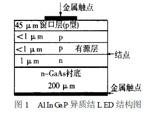
The standard Al InGaP L ED has a maximum current intensity of 50 mA at the junction, compared to 30 mA for conventional L ED technology. High current densities can cause local overheating, which can damage the crystal structure of the LED substrate. In these areas, dark spots are formed and no longer emit light, which degrades the performance of L ED . The active layer of the heterostructure can withstand higher current densities and reduce the possibility of impaired L ED performance.
A 45 μm thick GaP layer is placed over the three-layer Al InGaP layer as an interface to the metal. Most of the surface of the Al InGaP substrate is free of metallic materials, and only the 3 μm Al InGaP layer has aluminum on the side. Therefore, in a humid environment, there is almost no surface that will be oxidized. Al InGaP technology demonstrates its superior attenuation resistance under a variety of harsh conditions such as high drive currents, sudden temperature changes and humidity.
There are two main types of substrate materials for Al InGaP: absorption of light by a GaAs substrate, and absorption of photons generated in the active layer when it reaches the GaAs substrate, so the technique is called AS-Al InGaP technology; A process called "chip coupling" that replaces the absorbed GaAs substrate with a transparent GaP substrate (see Figure 2), a technique known as TS-Al InGaP technology. Applying a reflective film behind the GaP substrate, the photons are reflected back to increase efficiency, which is about twice the efficiency of AS-Al InGaP L ED.

In terms of increasing the light output of the chip, people's research is not only to change the amount of impurities in the material, lattice defects and dislocations to improve internal efficiency, but also how to improve the chip structure and increase the probability of photon emission inside the chip. The problem. Since the refractive index of the semiconductor material is greater than that of air, partial photons will undergo total reflection when they reach the chip interface. The traditional chip is usually a cube, and the chip is like a totally reflective right-angle prism. Part of the photon is reflected multiple times inside the crystal, and eventually it is lost due to the absorption of the crystal, and the crystal cannot be escaped. Therefore, even if many photons can be generated inside the chip, such as the inability to effectively increase the escape rate, the effect of increasing the luminous efficiency of the LED cannot be well reflected. Lumileds uses a chip structure with a trapezoidal cross-section (as shown in Figure 3), which allows more photons to exit in the direction of the bevel, greatly increasing the photon escape rate.
