
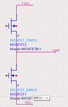
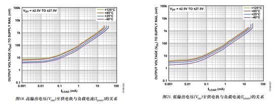
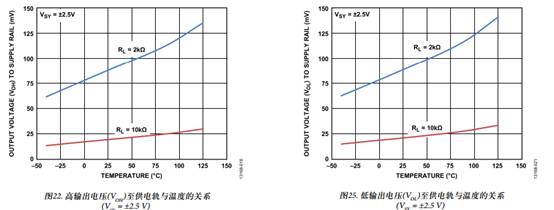
Since MOS transistors have an on-resistance, when current flows through them, a voltage drop occurs. This means that the higher the load, the greater the voltage drop in the on-state, and the harder it becomes for the output voltage to reach the power supply rail.
Therefore, even a rail-to-rail op amp may not be able to fully drive the output to the power supply level. When using such devices, it's important to consider the relationship between the load, temperature (which affects the on-resistance), and how much the output can actually reach.
2. Input bias current of the op amp cannot be ignored
A voltage divider circuit was designed, expecting an input of 1V to result in an output of 2V. However, during testing, there was always an offset of more than 6.7 mV. This deviation was significant enough to cause problems when feeding into a 12-bit ADC with a 3V range, leading to errors exceeding 600 counts. What could be the issue?
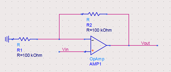
The positive and negative inputs of the op amp generate input bias currents due to TVS leakage and internal transistor characteristics. These currents are not equal, as no two devices are identical. The mismatch causes a bias voltage across external resistors, which gets amplified and introduces an error at the output. Choosing a BJT-based op amp, which typically has a high input bias current, can make this error even worse. As shown in the figure, this kind of op amp is "big but awkward," struggling to maintain accuracy.

Assuming the input bias currents are equal, the calculation simplifies. For the non-inverting input, the bias current results in nearly zero voltage, while for the inverting input, the bias current creates a voltage of about 350mV (when Vout is grounded, effectively R1 || R2). To compensate, a resistor should be added to the non-inverting input.


Even with a supply voltage change from 4.5V to 5.5V, the effect on the op amp’s output is only 10nV. However, this figure refers only to DC changes. AC variations, like ripple, can significantly degrade performance. In real-world applications, especially with switching power supplies, poor decoupling and filtering can lead to serious signal integrity issues. The PSRR (Power Supply Rejection Ratio) of the same op amp drops dramatically under AC conditions, making it unsuitable for precision applications.
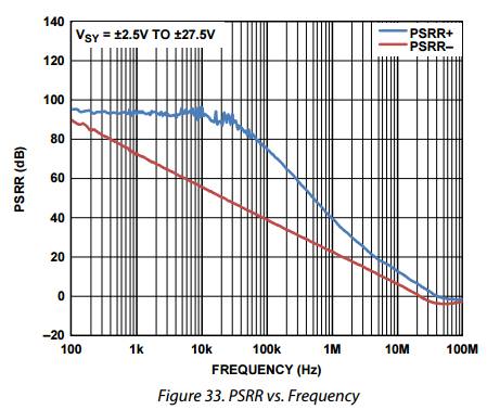
For example, a 500kHz ripple of 100mV can result in an output error of 0.3mV, which is often unacceptable for small-signal acquisition. In some cases, engineers add low-pass filters at the op amp’s power pin, though they must carefully consider resistor power ratings and thermal noise.
4. Compensation Capacitor of the Op Amp
In the past, I was told that adding a capacitor to the feedback loop would prevent oscillation. Following this advice, I added capacitors to every circuit, thinking I was being careful. But one day, I tried amplifying a 100kHz signal and noticed strange behavior. The capacitor introduced a low impedance path at that frequency, causing unexpected gain changes.
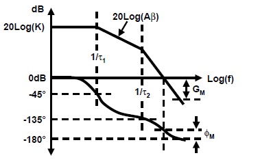
The key question: Do you really need a compensation capacitor? An op amp has an internal pole, causing a phase shift of up to -90°. Adding another pole (from a feedback capacitor) can increase the phase shift further, potentially leading to instability. If the loop gain Aβ reaches 1 at a phase of -180°, the circuit will oscillate. A compensation capacitor introduces a zero to stabilize the phase, but if the internal phase margin is already sufficient, additional compensation might not be needed.

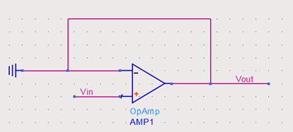
For a follower circuit, the output follows the input, but if the input approaches the power supply rails, the op amp may not operate linearly. This is because the internal transistors enter saturation or reverse bias, causing distortion or clipping.
6. The Slew Rate of the Op Amp Cannot Be Ignored
When designing a 1pps driver circuit requiring a rise time of ≤5ns, the output from the FPGA was followed by an op amp, but the rise time didn’t meet the requirement. Why? Because the slew rate wasn’t considered. The slew rate is the maximum rate at which the output voltage can change in response to a step input. If the required rate exceeds the op amp’s capability, the output will be distorted.
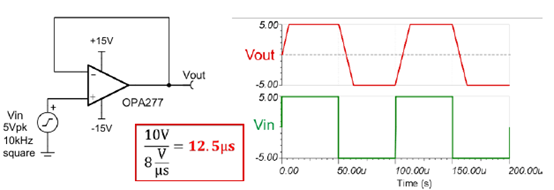
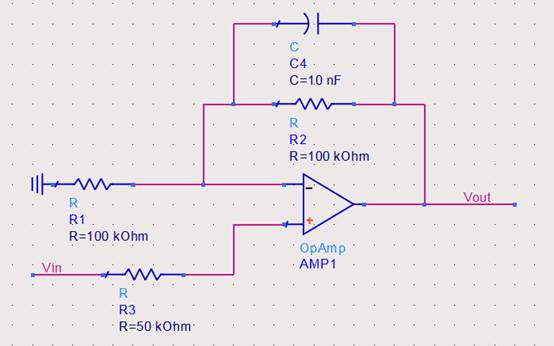
Checking the op amp’s specifications, it was clear that its slew rate was insufficient. At 5ns, it could only climb 20mV, far below what was needed. To fix this, a pulse boost circuit was added, using a differentiator and a DC resistor to sharpen the edge.
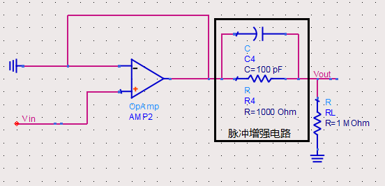
By combining a differentiating circuit (C4 and RL) with a DC resistor (R4), the rising edge was improved, allowing the signal to meet the design requirements.
7. Forgotten Feedback Resistor in Op Amp Circuits
To increase drive capability, a follower circuit was added at the end, using a current feedback amplifier (CFA). While simple, it turned out that without a feedback resistor, the circuit wouldn’t work properly. CFA and VFA (voltage feedback op amps) behave differently. The CFA model shows that the inverting input resistance is very small, and the open-loop gain is close to 1. Without a feedback resistor, the circuit fails to function as a follower.
Adding a feedback resistor ensures proper operation. This highlights the importance of understanding the differences between CFA and VFA models, as many engineers are more familiar with VFA examples.

8. The Instrument Amplifier’s Hidden Issue
A seemingly well-designed circuit with a 2x gain, 2V–10V input, and 1V–5V output appeared correct at first glance. However, at high input voltages, the circuit failed. The reason lies in the internal structure of the instrument amplifier. The actual output depends on internal nodes, and if the required voltage exceeds the power supply, the amplifier cannot function correctly.
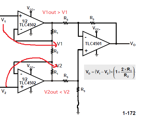
This shows that even a schematic that looks correct may have hidden issues related to internal voltage ranges and signal paths.
9. The Op Amp Slows Down ADC Sampling
An ADC was used to sample a signal, but the data was unstable when the signal changed rapidly. The ADC had a sampling time of 80ns, and the software engineer increased the number of samples, yet the problem persisted. The hardware engineer claimed everything was fine. But the root cause was the op amp’s delay and settling time.
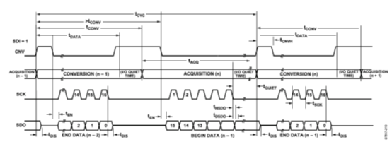
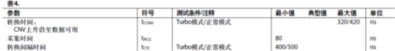
The op amp doesn’t respond instantly; it takes time to settle. With PCB layout and parasitic capacitance, the settling time increases, leading to larger errors. In a 16-bit ADC, a 0.4mV error could translate to several code words. Adjusting the sampling rate and increasing the acquisition time helped resolve the issue.
10. Overlooking Power Consumption of the Op Amp
After designing a board with strict power constraints, the calculated power consumption seemed acceptable. However, after testing, the actual power usage exceeded expectations. The mistake was in ignoring the power dissipated by the op amp itself—specifically, the voltage difference between the supply and the output. This led to unexpected power consumption, which was resolved by reducing the supply voltage in a later version.
Graded Radiator,Transformer Graded Radiators,Transformer Cooling Graded Radiator,Weather Proof Graded Radiator
Shenyang Tiantong Electricity Co., Ltd. , https://www.ttradiator.com